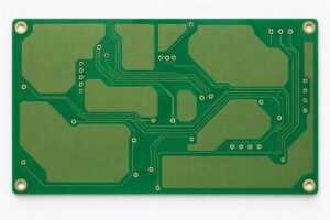
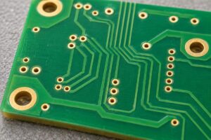
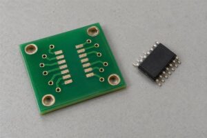
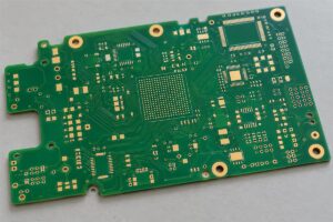
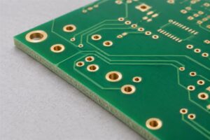
Thick Film Ceramic Circuit: Process, Design, and RFQ Guide
Do not choose a thick film ceramic circuit just because you need “a PCB that handles heat.” That description is too vague. Thick film is a specific additive metallization process: functional pastes are printed onto a ceramic substrate and fired to form conductors, resistors, dielectrics, or other features. It is valuable when its materials, geometry, firing sequence, assembly method, and reliability targets are designed as one system.
A thick film ceramic circuit is typically made by screen-printing conductive, resistive, and dielectric pastes onto an alumina or other compatible ceramic substrate, drying each print, and firing it according to the paste system. It suits hybrid circuits, sensors, heaters, power controls, LED products, and harsh-environment electronics that benefit from ceramic stability and printable functional layers.

What Is a Thick Film Ceramic Circuit?
The word “thick” describes the deposited functional film relative to thin-film vacuum deposition; it does not mean the ceramic board itself must be unusually thick. The fired circuit layer is created from formulated paste, not from patterned copper foil laminated to an FR-4 core.
| Element | Typical role | Design consequence |
|---|---|---|
| Ceramic substrate | Mechanical support, insulation, heat spreading | Material grade, thickness, flatness, finish, and strength matter |
| Conductor paste | Interconnects, pads, terminations | Metal system must match firing and attachment processes |
| Resistor paste | Printed resistive elements | Geometry, sheet resistance, firing, and trim strategy set final value |
| Dielectric/overglaze | Insulation, crossovers, protection | Pinholes, overlap, firing compatibility, and environment matter |
| Termination/plating | Soldering, wire bonding, brazing, or contact surface | Finish must match assembly and storage requirements |
Most thick-film substrates are alumina because it offers a practical balance of electrical insulation, mechanical stability, process compatibility, availability, and cost. That does not make all alumina grades interchangeable. Surface condition, purity, dimensions, porosity, and compatibility with the selected ink system can change print definition and adhesion.
Thick Film Is Not the Same as Thin Film, DBC, or LTCC
These technologies can all produce ceramic circuits, but they solve different problems. Choosing by thermal conductivity alone is a shortcut that often fails.
| Technology | How conductors are formed | Strong fit | Main limitation to examine |
|---|---|---|---|
| Thick film | Paste is printed and fired | Hybrid circuits, printed resistors, sensors, heaters, cost-effective repetition | Printed geometry and fired-paste properties |
| Thin film | Metal is deposited, patterned, and often plated | Fine geometry, precision RF, high-density interconnect | Cost, surface preparation, and process complexity |
| DBC/DCB | Thick copper is directly bonded to ceramic | High-current power modules and strong lateral heat spreading | Copper/ceramic stress and patterning limits |
| DPC | Metal is deposited and plated on ceramic | Finer features with engineered copper thickness | Plating control and supplier-specific capability |
| LTCC | Printed green ceramic layers are stacked and co-fired | Multilayer 3D interconnect, embedded passives, RF packaging | Shrinkage, material system, tooling, and NRE |
Kyocera describes screen printing as applying conductive paste through openings in a screen, while its thin-film processes use methods such as vacuum deposition or sputtering for very fine patterns. That process distinction should drive the selection.

How the Thick Film Process Works
The exact firing profile and sequence belong to the qualified material system. Still, the manufacturing flow is predictable enough to guide design review.
| Process step | What happens | What can go wrong |
|---|---|---|
| Substrate preparation | Ceramic is cleaned and inspected | Contamination, particles, chips, or wrong surface condition reduce yield |
| Screen/stencil setup | Pattern openings define the printed feature | Artwork compensation or screen condition is incorrect |
| Paste printing | Squeegee transfers paste to the substrate | Smear, skips, poor edge definition, or thickness variation |
| Drying | Solvent is removed before firing or overprinting | Trapped solvent, movement, contamination, or incomplete drying |
| Firing | Organic vehicle burns out and functional material bonds/forms | Profile mismatch, warpage, adhesion loss, or resistance shift |
| Repeat layers | Additional conductor, resistor, or dielectric prints are added | Registration and material compatibility accumulate risk |
| Trimming/finishing | Resistors may be laser-trimmed; finishes or singulation follow | Trim stability, damage, debris, or termination incompatibility |
| Inspection/test | Geometry, adhesion, resistance, electrical and visual results are checked | Test method does not match the actual failure mode |
Fewer print/fire cycles can reduce cost and process interaction, but consolidating layers is not always possible. Ask the manufacturer to review the sequence before freezing artwork.
Start With the Substrate, Not the Artwork
Designers often send a finished conductor pattern and treat the ceramic as a blank rectangle. That misses the substrate conditions that control registration, feature position, break strength, mounting, and assembly.
| Substrate input | Why it matters | What to put on the drawing/RFQ |
|---|---|---|
| Material and grade | Affects electrical, thermal, mechanical, and printing behavior | Supplier grade or agreed property set |
| Thickness | Affects stiffness, heat path, hole capability, and handling | Nominal and tolerance |
| Size and shape | Drives tooling, array utilization, and edge condition | Finished outline, datums, and tolerances |
| Surface finish | Influences print quality, adhesion, and thin/fine features | As-fired, lapped, or polished as required |
| Flatness/warp | Affects printing, component attachment, and fixture contact | Measurement method and limit |
| Holes/slots/scribes | Influence strength, registration, and singulation | Geometry, position, edge quality, and post-fire state |
| Edge/chip criteria | Ceramic is brittle | Inspection zone and allowable defect criteria |
CoorsTek publishes separate thick-film substrate design guidance because substrate tolerances, hole sizes, surface quality, and inspection conditions depend on grade, thickness, size, and manufacturing method. Use such values as supplier capability references, not universal ceramic rules.

Design Conductors for the Printing Process
The common mistake is copying an FR-4 copper layout onto ceramic and shrinking it until it fits. Printed paste has its own line definition, edge profile, fired thickness, resistivity, adhesion, and registration behavior.
| Layout feature | Design concern | Better action |
|---|---|---|
| Line width/space | Printing and firing change the achievable geometry | Use the selected supplier’s qualified design rules |
| Corners | Sharp geometry can print unevenly and concentrate current | Use smooth transitions where electrical function permits |
| Large metal areas | Paste thickness and firing stress may vary across area | Segment or redesign with manufacturer input |
| Pad size | Attachment method and print registration need margin | Define solder, braze, epoxy, or wire-bond process first |
| Crossovers | Dielectric integrity and overlap control are critical | Specify layer order, overlap, and electrical test |
| Edge clearance | Singulation, edge chips, and handling threaten conductors | Keep functional features outside agreed exclusion zones |
| High current path | Fired paste resistance and temperature rise may dominate | Calculate loss using actual fired conductor data |
Request a ceramic circuit DFM review before releasing fine geometry. The review should use the actual paste, screen, substrate, and firing capability—not a generic web table.
Printed Resistors Need a Complete Tolerance Budget
Integrated resistors are a major reason to select thick film, but “print a 10 kΩ resistor” is not a production specification. Final value depends on resistor composition, sheet resistance, geometry, termination interaction, firing, substrate, trim design, and environmental stability.
| Resistor decision | Question to resolve | Risk if omitted |
|---|---|---|
| Paste family/sheet resistance | Which qualified material covers the value range? | Poor geometry or excessive sensitivity |
| Aspect ratio | Is the length-to-width ratio practical? | Yield and trim range suffer |
| Initial tolerance | What result is expected before trimming? | Supplier and customer price different processes |
| Final tolerance | Is laser trimming required? | Cost or accuracy assumption is wrong |
| Power/load | What temperature rise and stability are allowed? | Drift or localized overheating |
| TCR and environment | What operating range and atmosphere apply? | Circuit meets room test but drifts in service |
| Trim geometry | Where may the cut go without creating a weak hotspot? | Unstable or damaged resistor |
Do not specify a tighter final tolerance than the circuit needs. It may force trimming and extra test steps without improving system performance.
Match Metallization to Assembly
A conductor that prints well is not automatically suitable for soldering, wire bonding, conductive adhesive, brazing, or repeated thermal cycling. Assembly must be defined before the metallization stack.
| Attachment method | Key compatibility checks | Typical documentation need |
|---|---|---|
| Soldering | Finish, wetting, leaching resistance, thermal profile | Solder alloy, flux, profile, joint criteria |
| Wire bonding | Surface metal, cleanliness, roughness, bond window | Wire alloy/diameter and pull/shear requirements |
| Conductive adhesive | Surface chemistry, cure, contact resistance | Adhesive, cure profile, aging requirement |
| Die attach | Flatness, metallization, thermal path, void control | Die material, attach system, inspection method |
| Mechanical contact | Wear, oxidation, contact force | Finish thickness and environmental exposure |
The same drawing should also state whether parts will be supplied as individual substrates, snap arrays, scribed sheets, or processed assemblies. That choice affects handling, print registration, component placement, and final singulation.
Where Projects Commonly Get Stuck
In engineering forums and supplier discussions, three patterns recur. The pain is yield loss discovered after screens and tooling are made. The technical difficulty is balancing printable geometry, electrical resistance, thermal behavior, and brittle ceramic mechanics. The decision barrier is that buyers compare quotes without realizing the suppliers assumed different substrate grades, paste systems, inspection, trimming, and test coverage.
| Quote difference | What may actually be different | Clarifying question |
|---|---|---|
| Lower tooling charge | Simpler screen set or customer-owned tooling assumption | What tooling, artwork conversion, and revisions are included? |
| Lower unit price | Fewer prints/fires, looser inspection, or larger lot | Which operations and acceptance tests are included? |
| Shorter lead time | Stock substrate and standard paste system | Are the specified material and finish genuinely matched? |
| Better stated tolerance | Different measurement method or post-trim value | Is the tolerance before or after trim, and under what conditions? |
| “Equivalent” material | Different ceramic or paste family | Which properties and qualification evidence define equivalence? |
A useful PCB and ceramic substrate engineering review should normalize those assumptions before price comparison.
Save This Thick Film Ceramic Circuit RFQ Table
| RFQ category | Information to provide | Why suppliers need it |
|---|---|---|
| Application | Function, environment, reliability level, expected life | Guides material and validation choices |
| Substrate | Material/grade, size, thickness, flatness, surface, holes | Establishes the physical platform |
| Circuit layers | Conductor, resistor, dielectric, overglaze, backside features | Defines print/fire sequence |
| Electrical | Netlist, resistance targets, current, voltage, isolation | Sets material and test needs |
| Assembly | Solder, bond wire, die attach, adhesive, operating profile | Determines metallization and finish compatibility |
| Tolerances | Geometry, registration, resistor value, critical dimensions | Separates functional needs from preferences |
| Test/inspection | Visual criteria, electrical tests, adhesion, trim, sampling | Defines acceptance and cost |
| Delivery form | Singles, arrays, scribed panels, packaging, traceability | Controls handling and downstream automation |
| Volume | Prototype, annual demand, lot size, forecast | Supports tooling and process selection |
Submit native drawings, layer identification, and a controlled requirement list when requesting ceramic PCB fabrication support. A screenshot cannot define registration, paste identity, firing order, or test limits.
FAQ
What is a thick film ceramic circuit?
It is a circuit formed by printing functional pastes—such as conductors, resistors, and dielectrics—onto a ceramic substrate and firing them to create stable electrical features.
Is thick film the same as thick copper ceramic PCB?
No. “Thick film” refers to printed and fired paste technology. Thick-copper technologies such as DBC use a substantially different metallization structure and process.
What ceramic is commonly used for thick film circuits?
Alumina is the common workhorse because of its availability, insulation, stability, and compatibility with established thick-film systems. The exact grade must match the printing and application requirements.
Can thick film circuits include printed resistors?
Yes. Printed resistors are a key advantage. Their value and stability require a controlled paste family, geometry, firing process, tolerance plan, and often laser trimming.
When should I choose thin film instead?
Consider thin film when the design requires finer geometry, tighter pattern precision, or performance that the selected thick-film process cannot reliably achieve. Compare complete supplier capabilities rather than choosing by the technology name alone.
Final Takeaway
A thick film ceramic circuit is not simply artwork printed on a heat-resistant board. It is a matched system of ceramic, paste, screen printing, firing, finishing, assembly, and test. Start with electrical and environmental requirements, select the material system with the manufacturer, then design within verified process rules. Save the RFQ table above; it will expose most hidden differences before tooling begins.