Standard PCB Thickness: 1.6 mm, Tolerances, and Stackup Selection
The usual answer to “What is the standard PCB thickness?” is 1.6 mm. That answer is useful for a rough enclosure model—and risky everywhere else. A 1.6 mm nominal board can still fail a card-edge connector, miss an impedance target, bow in reflow, or collide with a housing if nobody defines finished thickness and tolerance.
There is no single thickness that every PCB must use. The right value comes from the electrical stackup, mechanical interface, fabrication process, assembly load, and procurement drawing.

Direct Answer: What Is the Standard PCB Thickness?
1.6 mm (about 0.063 in) is the most common nominal thickness for general rigid PCBs, but it is not a universal mandatory standard. Common alternatives include 0.4, 0.6, 0.8, 1.0, 1.2, 2.0, 2.4, and 3.2 mm. Specify finished board thickness and tolerance based on stackup, connector fit, impedance, rigidity, weight, and manufacturing capability.
1. Treat 1.6 mm as a Default, Not a Design Rule
| Statement | Engineering verdict | Better interpretation |
|---|---|---|
| “All standard PCBs are 1.6 mm” | False | 1.6 mm is a widely stocked general-purpose nominal |
| “Four layers require 1.6 mm” | False | Layer count and total thickness are separate choices |
| “Board thickness equals core thickness” | False | Finished thickness includes the laminated construction and outer features |
| “The fabricator will choose the tolerance” | Risky | Put the required finished limit in procurement data |
| “A thinner board is always cheaper” | False | Nonstandard material, handling, yield, and panel support can reverse the saving |
| “Thicker means more reliable” | Incomplete | Via aspect ratio, thermal mass, stress, and connector fit may get worse |
IPC-2221C is the current generic printed-board design standard, while IPC-6012F establishes performance requirements for rigid printed boards. Neither turns one popular nominal into the correct thickness for every product.
2. Use Common Thicknesses as a Sourcing Map
| Nominal thickness | Where it is often considered | Main design concern |
|---|---|---|
| 0.4 mm | Modules, compact devices, special thin products | Handling, bow, assembly support, via geometry |
| 0.6 mm | Small modules and space-constrained assemblies | Stiffness and process capability |
| 0.8 mm | Compact products, daughtercards, some connector-defined designs | Mechanical fit and reflow support |
| 1.0 mm | Thin industrial/consumer boards | Stackup availability and rigidity |
| 1.2 mm | Moderate thickness reduction | Connector and enclosure assumptions |
| 1.6 mm | General rigid PCB default | Do not assume tolerance or stackup |
| 2.0 mm | Added stiffness or stackup space | Via aspect ratio and connector compatibility |
| 2.4 mm | Structural/power/special boards | Material availability and thermal mass |
| 3.2 mm | Heavy structural or specialized assemblies | Drilling, plating, assembly, weight, cost |
This is a planning table, not a factory capability promise. Stocked constructions, minimum order economics, and tolerances vary with material family, layer count, copper, panel format, and supplier.
3. Specify Finished Thickness, Not a Vague Laminate Number
| Term | What it means | Why confusion happens |
|---|---|---|
| Core | Cured copper-clad laminate used inside the stack | Designers sometimes call it “the board thickness” |
| Prepreg | Uncured resin/glass material pressed between layers | Final thickness depends on glass style, resin flow, and copper pattern |
| Dielectric thickness | Separation between selected copper layers | Used for impedance and field modeling |
| Stackup thickness | Sum of stack materials in the construction model | May be nominal or calculated before pressing |
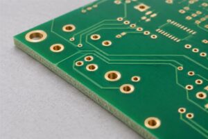
| Finished board thickness | Measured completed PCB thickness under an agreed method | The dimension that must fit the product |
| Local thickness | Thickness at a specified area | Copper, plating, mask, or topology can affect measurement |
On the fabrication drawing, write something like “finished board thickness: X mm ± Y mm” and define any critical local measurement area. Do not expect a note saying “FR-4, 1.6 mm” to resolve every interpretation.

4. Build Thickness from the Electrical Stackup
| Stackup input | Thickness effect | Electrical consequence |
|---|---|---|
| Core and prepreg selection | Sets dielectric spacing and total build | Changes impedance and coupling |
| Copper weight/thickness | Adds physical thickness and affects resin fill | Changes conductor geometry and loss |
| Glass style/resin content | Changes pressed dielectric thickness | Alters effective Dk and impedance |
| Plane distribution | Affects copper balance during lamination | Influences warp and dimensional behavior |
| Sequential lamination | Adds construction cycles and material constraints | Enables HDI but complicates tolerance |
| Controlled-impedance target | May force specific dielectric distances | Can override the preferred total thickness |
Do not select total thickness first and squeeze every dielectric until the number fits. Start with routing, reference planes, impedance, isolation, via structure, and manufacturable materials; then close the total-thickness target with the fabricator.
5. Understand Why Finished Thickness Varies
| Variation source | What changes | Control method |
|---|---|---|
| Laminate sheet tolerance | Core starting thickness | Use controlled material callout and supplier data |
| Prepreg resin flow | Pressed dielectric thickness | Select glass/resin system and model copper distribution |
| Inner-layer copper density | Local resin consumption | Balance copper or add thieving where appropriate |
| Copper/plating | Outer and hole-wall buildup | Define finished copper requirements |
| Solder mask | Small local surface contribution | Define measurement method if mechanically critical |
| Press cycle | Resin flow and final consolidation | Qualified process and stackup |
| Measurement location/method | Reported result | Agree tool, pressure, location, and inclusions |
The tolerance must be realistic for the entire construction. Tightening it without a mechanical reason can reduce material options, complicate pressing, increase sorting, and add cost without improving product performance.
6. Let Connectors Set the Limit When They Must
Card-edge connectors, press-fit systems, board-in connectors, guides, and slots may have a narrow board-thickness window. In these cases, connector fit outranks the generic 1.6 mm habit.
| Interface | Thickness question | Evidence required |
|---|---|---|
| Card-edge connector | What finished board range does the contact accept? | Connector drawing and PCB bevel/finish requirement |
| Board-in connector | What board thickness and insertion tolerance apply? | Exact manufacturer specification |
| Press-fit connector | Does stack thickness support pin geometry and process? | Connector application specification |
| Enclosure guide/slot | What is the complete mechanical tolerance stack? | Housing drawing and worst-case analysis |
| Standoff/screw stack | Will board thickness alter preload or alignment? | Mechanical assembly model |
| Mating daughterboard | Do connector heights and parallelism close? | 3D model and datum plan |
USB-IF specifications also demonstrate why interface-specific documents matter: defined test fixtures and connector systems can prescribe PCB dimensions that differ from the common 1.6 mm assumption. Always follow the exact interface specification used by the product.
7. Check Via Aspect Ratio Before Making the Board Thicker
| Change | Potential benefit | New risk |
|---|---|---|
| Increase total thickness | More stiffness or dielectric spacing | Higher through-hole aspect ratio |
| Reduce drilled hole diameter | Saves routing space | Harder drilling/plating and reliability margin |
| Add more layers | More routing/planes | Thicker build or thinner dielectrics |
| Use blind/buried vias | Reduces full-depth via burden | Sequential lamination cost and process complexity |
| Use microvias | Enables HDI routing | Structure, stacking, and reliability constraints |
| Increase finished hole | Easier plating geometry | Larger pads and routing keepouts |
Aspect ratio is based on the relevant hole depth and drilled diameter, not a casual finished-hole estimate. A thicker board can turn an otherwise ordinary via into a more demanding fabrication feature.
8. Balance Rigidity Against Assembly Risk
| Board condition | Thin-board concern | Thick-board concern |
|---|---|---|
| SMT printing | Support and coplanarity | Stencil separation over local warp |
| Pick-and-place | Panel vibration/flex | Usually stable, but heavier panels load handling |
| Reflow | Sag, bow, component strain | Greater thermal mass and temperature lag |
| Depaneling | Flex damage near components | Higher separation force |
| Hand assembly | Easy bending | More heat required at large copper features |
| Field use | Mechanical flex/fatigue | Weight and rigid stress transfer |
Panel rails, breakaways, fixtures, copper balance, component placement, and reflow profile can matter as much as nominal board thickness. Ask the assembler about handling the real panel, not only the individual PCB.

9. Do Not Use Thickness Alone to Solve Thermal Problems
| Thermal objective | More effective variables | Role of total board thickness |
|---|---|---|
| Spread component heat | Copper planes, thermal vias, coins, heat spreaders | Only one part of the path |
| Lower junction temperature | Interface, airflow, heatsink, copper connection | Extra dielectric may add resistance |
| Carry higher current | Finished copper, width, temperature rise | Board thickness alone adds no conductor area |
| Improve power-cycle reliability | CTE match, via structure, material, strain | Can help or hurt depending on construction |
| Insulate electrically | Material CTI, dielectric thickness, spacing | Total thickness is not the same as required insulation path |
A 2.0 mm FR-4 board is not automatically a better thermal board than a well-designed 1.0 mm construction. Model the actual heat path.
10. Release a Stackup That CAM Can Build
| Required item | Why manufacturing needs it | Weak alternative |
|---|---|---|
| Finished thickness and tolerance | Defines product acceptance | “Standard thickness” |
| Layer count and order | Establishes physical construction | Copper files without stack order |
| Copper requirements | Controls conductor and plating build | “1 oz” without finished/starting context |
| Material family/performance | Controls electrical, thermal, and compliance needs | Brand name without grade or property target |
| Impedance table | Connects geometry to dielectric construction | Trace widths only |
| Via structure | Sets drilling and lamination sequence | Drill file without span definition |
| Critical mechanical areas | Protects connectors, slots, edges, and contacts | One global note for local constraints |
| Approved stackup | Locks the quoted construction | Unrecorded email assumption |
An early PCB stackup and DFM review should happen before routing is frozen. If the fabricator changes dielectric thickness after layout, controlled impedance and via geometry may both need revision.
11. Choose PCB Thickness with This Decision Table
| Priority | Question | Selection direction |
|---|---|---|
| Fixed interface | Does a connector or slot prescribe thickness? | Use its allowed finished range first |
| Enclosure | What are worst-case clearances and datums? | Close mechanical tolerance stack |
| Electrical | What dielectric spacing supports impedance and isolation? | Build a realizable stackup |
| Vias | Can holes be drilled and plated at the selected depth? | Adjust thickness, hole size, or via technology |
| Assembly | Can the panel survive printing, placement, and reflow? | Add support or revise construction |
| Environment | What shock, vibration, temperature, and humidity apply? | Validate material and mechanics |
| Supply | Is the construction stocked and repeatable? | Prefer qualified common materials where possible |
| Cost | Which choice reduces total—not only laminate—cost? | Include process, panel utilization, test, and yield |
For a simple unconstrained board, 1.6 mm is a sensible quotation baseline. For anything connector-controlled, impedance-sensitive, unusually thin/thick, HDI, high-layer-count, or mechanically loaded, decide with the fabricator rather than by habit.
12. Standard PCB Thickness Release Checklist
| Check | Pass condition | Stop condition |
|---|---|---|
| Finished nominal | Explicitly stated in mm | “Standard” only |
| Tolerance | Functional and manufacturable | No limit or arbitrary tight limit |
| Measurement | Location/inclusions defined when critical | Connector fit depends on an undefined reading |
| Stackup | Materials, copper, and dielectric values approved | Total thickness entered without construction |
| Impedance | Solver/fabricator stackup aligned | Nominal Dk and guessed dielectric |
| Connector fit | Exact component drawing checked | 1.6 mm assumed from memory |
| Via geometry | Aspect ratio/process reviewed | Drill size chosen after thickness freeze |
| Assembly | Panel stiffness and thermal behavior reviewed | Thin/thick board sent without line input |
| Documentation | Drawing, data, quote, and order agree | Conflicting thickness values |
Frequently Asked Questions
Is 1.6 mm the standard PCB thickness?
It is the most common general-purpose nominal for rigid PCBs, but it is not mandatory for every design. Connector fit, stackup, impedance, stiffness, enclosure space, and fabrication capability can justify another value.
Does solder mask count in PCB thickness?
It can affect a local physical measurement, but procurement conventions and measurement methods vary. If total thickness is mechanically critical, state whether coatings and local copper features are included and define where the board is measured.
What tolerance should I use for PCB thickness?
Use the widest tolerance that still satisfies the product, then confirm it against the exact construction and applicable procurement standard. Do not copy one percentage to every thin, thick, connector-controlled, or unusual board.
Does a thicker PCB carry more current?
Not by itself. Current capacity is driven mainly by conductor cross-section, allowable temperature rise, copper environment, and heat removal. Increasing dielectric or core thickness without increasing copper does not automatically raise current capacity.
Can a four-layer PCB be 0.8 mm thick?
Yes, if a manufacturable four-layer stackup meets dielectric, copper, impedance, via, bow, and assembly requirements. Confirm actual material availability and tolerance through a PCB fabrication engineering review before completing the layout.
Final Takeaway
The standard PCB thickness is best understood as a sourcing convention: 1.6 mm is common, not compulsory. Specify the finished value and tolerance that the product actually needs, then prove that the stackup, vias, impedance, connectors, enclosure, panel, and assembly process all support it. A controlled PCB manufacturing stackup is more valuable than a familiar number with no tolerance or construction behind it.