PCB Testing Guide: 12 Methods, Coverage Gaps, and Test Strategy
The most expensive PCB test is not always the one with the costly fixture. It is the test that passes boards without detecting the defect that matters—or fails good boards until operators learn to press “retest.” More equipment does not automatically create more confidence. Good coverage comes from matching each likely failure to a method that can actually see it.
This guide separates bare-board testing from PCBA testing, compares 12 common methods, and shows how to build a test flow for prototypes, NPI, and volume production.

Direct Answer: Which PCB Test Should You Use?
Use bare-board continuity and isolation testing to find open and shorted copper networks. Add physical inspection for dimensions, plating, solder mask, and internal structure. On assembled boards, combine SPI/AOI or X-ray with flying probe, ICT, or boundary scan for assembly defects, then use functional test for powered behavior. Select the combination from defect risk, physical access, volume, diagnostic needs, and cost.
1. Define the Product Under Test Before Choosing Equipment
“Test the PCB” can refer to an empty board, an assembled board, or a complete product. Those stages do not share the same reference data or failure mechanisms.
| Product under test | Main reference | Typical defect question | Suitable test family |
|---|---|---|---|
| Bare PCB | Fabrication data and netlist | Is the copper network and board construction correct? | Electrical, optical, dimensional, structural |
| PCBA before power | BOM, placement and assembly drawings | Are the right parts and solder joints present? | SPI, AOI, X-ray, flying probe, ICT |
| Powered PCBA | Schematic, firmware and test specification | Do rails, clocks, interfaces and functions operate within limits? | Boundary scan, programming, functional test |
| Complete product | System requirements and risk controls | Does it work safely under intended conditions? | System, compliance, environmental and reliability test |
Do not accept “100% tested” until the supplier names the product stage, coverage, limits, and recorded result.
2. Match the Defect to the Test—Not the Other Way Around
This is the table worth saving. Start with the defect you cannot afford to ship, then choose prevention and detection controls.
| Defect | Best early detector | Useful confirmation | Common coverage gap |
|---|---|---|---|
| Bare copper open/short | Bare-board electrical test | Netlist audit | Wrong reference netlist |
| Hole/slot out of tolerance | Dimensional inspection | Fit gauge or first article | Electrical test cannot see it |
| Weak plating/via structure | Process coupons and microsection | Reliability stress testing | A via can conduct today and fail later |
| Insufficient/excess paste | SPI | Post-reflow joint evidence | AOI after reflow cannot reconstruct print history |
| Wrong/missing component | AOI or ICT | Functional test | Hidden/ambiguous markings |
| BGA bridge/open | X-ray, boundary scan or electrical test | Functional test and process data | 2D overlap and inaccessible nets |
| Wrong resistor/capacitor value | ICT or flying probe where measurable | Functional response | Parallel circuit paths distort readings |
| Firmware/programming error | Readback, checksum and version control | Functional test | “Program succeeded” without version trace |
| Marginal analog performance | Functional/parametric test | Environmental characterization | Go/no-go digital test only |
| Intermittent connection | Stress, monitoring and fault localization | Failure analysis | One room-temperature pass |
One test rarely closes an entire row. The goal is complementary coverage, not duplicated cost.
3. Understand What Bare-Board Electrical Test Proves
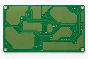
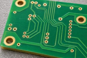
IPC-9252B covers electrical testing of unpopulated printed boards. Its scope is clear: electrical test verifies conductive networks against design requirements. It does not prove that the board can be assembled or that every physical customer requirement is satisfied.
| Bare-board approach | Where it fits | Cost/coverage behavior |
|---|---|---|
| Flying probe | Prototype, low volume, many revisions | Little dedicated fixture cost; longer unit time |
| Fixture/grid test | Stable higher volume | Higher tooling cost; fast repeated test |
| Continuity test | Every required net path | Detects opens using specified resistance limits |
| Isolation test | Required net-to-net combinations | Detects shorts/leakage using specified thresholds/voltage |
| Four-wire/Kelvin measurement | Selected low-resistance paths | Removes much lead/contact resistance from precision measurement |
Specify which netlist is authoritative, test voltage/current, continuity and isolation limits, test population, retest rules, and report format. “E-test passed” without those fields is weak traceability.
4. Add Physical Tests That Electrical Test Cannot Replace
| PCB characteristic | Practical evidence | Why it matters |
|---|---|---|
| Finished outline, holes and slots | Calibrated dimensional measurement | Mechanical assembly and connector fit |
| Copper geometry/registration | AOI and selected measurements | Current capacity, spacing and feature integrity |
| Plated hole and microvia structure | Coupon/microsection | Internal plating, registration and interface quality |
| Finished copper/finish thickness | Appropriate measurement such as microsection or XRF | Reliability, solderability or contact requirements |
| Solder mask and legend | Visual/optical inspection and applicable tests | Pad exposure, dams, markings and insulation intent |
| Cleanliness/material behavior | Named IPC-TM-650 or customer method | Leakage, corrosion and reliability risk |
IPC-TM-650 is a library of methods, not one blanket acceptance standard. Always call out the method number, revision, specimen, conditioning, sample plan and limit.

5. Use Inspection to Control the Assembly Process
Inspection is strongest when it catches the defect immediately after the process that created it.
| Method | Best timing | Strongest use | What it cannot guarantee |
|---|---|---|---|
| SPI | After paste print | Paste volume, height, area and offset trends | Final joint quality |
| Pre-reflow AOI | After placement | Missing, shifted, wrong-orientation parts | Reflow outcome |
| Post-reflow AOI | After soldering | Visible joints, polarity, presence and placement | Hidden bottom-side joints |
| 2D X-ray | After reflow | BGA bridges, missing balls, gross voids and hidden-joint patterns | Full depth separation or every crack |
| 3D X-ray/CT | NPI, sampling or complex failures | Spatial analysis of hidden structures | High-speed universal screening at no cost |
Inspection should feed process correction. If operators only repair individual boards while the printer, placement program, profile, or material remains unchanged, inspection becomes an expensive sorting station.
6. Choose Flying Probe or ICT by Economics and Access
| Decision factor | Flying probe | Fixture-based ICT |
|---|---|---|
| Upfront tooling | Lower | Higher |
| Program/revision flexibility | Strong | Fixture and program may need changes |
| Unit test time | Usually longer | Usually shorter |
| High-volume economics | Often weaker | Often stronger after tooling amortization |
| Physical access | Movable probes still need reachable targets | Dedicated probes need planned test points |
| Diagnostics | Good when the program isolates nets/components | Strong for modeled accessible faults |
Do not compare only fixture quotations. Compare expected volume, cycle time, labor, maintenance, false calls, revision life, diagnostics, and the cost of an escape.
7. Use Boundary Scan Where Physical Probes Cannot Reach
Boundary scan, commonly associated with JTAG/IEEE 1149.x, uses test functions inside compatible ICs to control and observe pins. It can test digital interconnects hidden under BGAs and nets without individual test points.
| Boundary-scan requirement | Design action | Failure if ignored |
|---|---|---|
| Supported devices and BSDL models | Confirm exact orderable parts early | Expected coverage does not exist |
| Complete TAP chain | Route TCK, TMS, TDI, TDO and required control correctly | Chain will not communicate |
| Stable power/reset/boot states | Provide deterministic fixture control | Devices enter the wrong mode |
| Accessible connector/pads | Reserve test interface and ground | Production cannot connect reliably |
| Coverage report | Map detectable opens/shorts and exclusions | “JTAG tested” remains an empty claim |
Boundary scan complements AOI, X-ray, ICT and functional test. It does not inspect solder shape or verify every analog function.
8. Build a Safe, Diagnostic Power-Up Sequence
| Power-up gate | Measurement | Stop rule |
|---|---|---|
| Before power | Rail-to-ground resistance, polarity and visible damage | Unexpected short or unresolved anomaly |
| Current-limited energization | Input current and initial rail response | Current limit, collapse or rapid temperature rise |
| Rail validation | Voltage, ripple, sequence and power-good | Any rail outside approved limits |
| Clock/reset validation | Frequency, amplitude and reset timing | Missing/unstable clock or incorrect reset release |
| Processor/firmware start | ID, boot log, checksum/version | Unknown or unapproved firmware |
| Subsystem activation | Enable loads/interfaces one at a time | Fault cannot be localized |
For high-energy, mains, battery, medical, automotive or other safety-relevant boards, use the approved product procedure and protective equipment. A generic bench sequence is not authorization to energize hazardous hardware.
9. Make Functional Test Quantitative
Functional test should stimulate inputs, load outputs, measure performance and store results. A green LED alone does not demonstrate margin.
| Test field | Required definition | Example failure in weak plans |
|---|---|---|
| Configuration | Hardware revision, firmware, calibration and options | Test runs with the wrong image |
| Conditions | Supply, load, temperature, warm-up and timing | Results vary by station/operator |
| Stimulus | Source, amplitude, sequence and tolerance | Unknown input accuracy |
| Measurement | Instrument, range, uncertainty and settling | No confidence near the limit |
| Limit | Upper/lower bounds and engineering rationale | “Looks normal” becomes acceptance |
| Data | Unit ID, station, program version and measured values | Pass/fail cannot support investigation |
NI’s production-test material emphasizes maintainable software-defined systems, consistency and throughput. Those benefits appear only when test definitions and configuration control are disciplined.
10. Do Not Confuse Production Test with Reliability Validation
Production test screens workmanship and verifies selected functions. Reliability testing asks whether the design/process survives defined stresses over time.
| Test class | Typical purpose | Production use |
|---|---|---|
| Thermal cycle/shock | Expose expansion-related interconnect weaknesses | Qualification, validation or controlled sampling |
| Vibration/mechanical shock | Evaluate mechanical and solder-joint robustness | Qualification or application-specific sampling |
| Humidity/SIR/CAF-related evaluation | Evaluate insulation and electrochemical risk | Process qualification/monitoring as justified |
| Power cycling | Stress power devices, joints and thermal interfaces | Validation and selected screening |
| HALT/HASS-style work | Discover margins or screen with a validated process | Never apply blindly as a generic “quality test” |
| Life/endurance test | Evaluate degradation under defined operating stress | Design validation and reliability program |
A unit passing functional test at room temperature is evidence of present function, not proof of service life.
11. Design for Test Before Routing Is Finished
During PCB manufacturing and test planning, review access while placement and stackup can still change.
| DFT checkpoint | Release requirement |
|---|---|
| Power and ground | Safe injection, measurement, fixture return and discharge paths |
| Critical analog nodes | Pads positioned to avoid loading sensitive signals during normal operation |
| Digital access | Test points or boundary-scan coverage with documented exclusions |
| Programming/debug | Stable connector/pads, keying and access after mechanical assembly |
| Test modes | Deterministic firmware and hardware control, including reset/boot straps |
| Fixtures | Probe keepouts, support, fiducials, panel rails and strain limits |
| Identification | Board serial/lot and revision readable by the station |
Test pads are not automatically harmless. Stubs, capacitance, spacing, creepage, RF behavior and mechanical access still need engineering review.
12. Select the Flow by Build Stage
| Build stage | Recommended baseline | Main objective |
|---|---|---|
| Prototype | Bare-board E-test, visual checks, controlled power-up, focused functional measurements | Learn quickly without expensive fixtures |
| Engineering validation | Broader parametric, environmental and corner testing | Prove requirements and margins |
| NPI/pilot | SPI/AOI/X-ray as applicable, flying probe/ICT trial, station correlation, defect logging | Stabilize process and test coverage |
| Volume production | Optimized inspection, ICT/boundary scan/functional flow, traceable data and SPC | Meet takt time without hiding escapes |
| High-reliability build | Contract-specific coupons, structural tests, traceability and reliability evidence | Control low-frequency, high-consequence failures |
Coordinate PCB fabrication and assembly testing using forecast volume, component technology, access, target cycle time, test limits and traceability—not the phrase “full test.”

PCB Test Release Checklist
| Gate | Pass condition | Blocker |
|---|---|---|
| Defect model | Credible defects map to prevention/detection controls | Equipment chosen without coverage logic |
| Controlled references | Netlist, BOM, CAD, firmware and drawings agree | Mixed or unknown revisions |
| DFT complete | Access, JTAG, programming, panel and support reviewed | Fixture assumptions made after layout |
| Methods/limits | Conditions, units, thresholds, sample plan and revisions stated | Generic “test per IPC” note |
| Station validation | Known-good and seeded/known-fault evidence challenge the program | Golden board merely passes itself |
| Measurement confidence | Calibration, uncertainty and guard-band policy are defined | Limits tighter than measurement capability |
| Data/traceability | Serial/lot, result, program and station are stored | Pass/fail cannot be reconstructed |
| Failure handling | Retest, repair, quarantine and escalation are controlled | Repeat-until-pass behavior |
| Change control | Coverage reviewed after design, BOM, firmware or process changes | Old program used by habit |
Before releasing tooling, request a final CAM, DFM, and testability review and store the coverage matrix with the manufacturing package.
Frequently Asked Questions
What is PCB testing?
PCB testing verifies a bare board or assembled PCBA against defined electrical, physical, workmanship and functional requirements. The product stage must be stated because bare-board and assembly tests find different defects.
Is bare-board electrical test enough?
No. It is essential for connectivity and isolation, but it does not prove dimensional accuracy, internal structural quality, solderability, assembly workmanship or circuit function.
Which is better: flying probe or ICT?
Flying probe is usually attractive for prototypes, changing designs and lower volumes. Fixture-based ICT generally offers faster repeated testing for stable higher volumes. Coverage and access still need comparison.
Can AOI detect BGA solder problems?
Conventional AOI cannot see most joints under a BGA. X-ray, boundary scan, electrical tests, process controls and functional tests provide complementary evidence.
What should a PCB test report include?
It should identify the unit/lot, design and program revisions, station, date, methods, conditions, measured results or controlled pass/fail evidence, limits, failures, retests, repairs and final disposition as required.
Final Takeaway
The right PCB test is a coverage system, not a machine. Define the product stage, list credible defects, design access early, combine complementary methods, use quantitative limits, and track failures back to process causes. That approach catches more real problems while reducing unnecessary tests and repeat-to-pass noise.