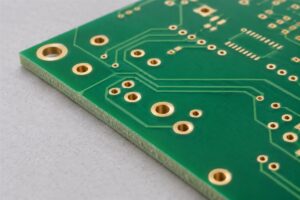
High-Speed PCB Manufacturing: Stackup, Impedance, Loss, and DFM Control
“Specify 50-ohm traces and let the fabricator adjust the width” is not a complete high-speed PCB manufacturing plan. It may produce an impedance coupon that passes while your routed channel has different copper density, via stubs, glass-weave exposure, solder-mask coverage, or launch geometry. Impedance matters. So do loss, skew, reference continuity, fabrication variation, and the exact method used to verify them.
Reliable high-speed PCB manufacturing begins before CAM compensation. The designer and fabricator must agree on the production stackup, materials, copper profile, finished geometry, via structures, coupon design, test method, tolerance, and change-control rules.

Direct Answer: What Is High-Speed PCB Manufacturing?
High-speed PCB manufacturing is the controlled fabrication of boards whose signal quality depends materially on transmission-line geometry, dielectric properties, conductor loss, reference planes, vias, and process tolerances. It requires a production-ready stackup, qualified materials, impedance and sometimes insertion-loss verification, precise imaging/etching, controlled drilling and plating, via-stub management, representative coupons, and as-built data—not merely narrow traces.
1. Define “High Speed” by Edge and Channel Risk
A low clock frequency can still produce transmission-line behavior when its edge is fast. A multi-gigabit interface adds insertion loss, return loss, crosstalk, skew, and via/connector discontinuities. Do not classify the board by marketing data rate alone.
| Signal condition | Manufacturing sensitivity | Evidence to define |
|---|---|---|
| Fast single-ended control/clock | Impedance, reference path and stub reflections | Edge rate, topology, layer and target impedance |
| Differential serial channel | Differential/common-mode impedance, loss and skew | Data rate, reach, channel budget and pair geometry |
| DDR/source-synchronous bus | Delay matching, impedance and reference transitions | Timing budget and tuning constraints |
| RF/microwave path | Dk/Df, copper profile, launches and finish | Frequency band, line type and S-parameter goal |
| High-current fast switching | PDN impedance, loop inductance and crosstalk | Current transient, edge, plane and return structure |
Send the channel requirements with the PCB package. “High speed” by itself gives CAM nothing measurable.
2. Freeze a Manufacturable Stackup Before Final Routing
The field solver uses dielectric thickness, Dk, copper thickness, trace geometry and solder-mask assumptions. If the fabricator later substitutes prepreg constructions or changes finished thickness, the routed width and spacing may no longer produce the intended impedance or loss.
| Stackup field | What must be controlled | Why it changes the channel |
|---|---|---|
| Material family | Named laminate/prepreg or approved equivalents | Dk, Df, thermal and processing behavior vary |
| Core/prepreg construction | Glass style, resin content and ply count | Controls thickness, effective Dk and weave exposure |
| Finished dielectric thickness | Target and tolerance after lamination | Directly changes trace-to-plane coupling |
| Copper | Starting/finished thickness and foil profile | Changes geometry and conductor loss |
| Layer function | Signal/reference/power assignments | Determines return path and crosstalk |
| Solder mask | Covered/exposed assumption and actual material | Changes effective impedance on outer layers |
| Overall board thickness | Finished target/tolerance | Affects connectors, vias and mechanical fit |
During an early high-speed PCB manufacturing review, route against the fabricator’s producible stackup—not a generic CAD template.
3. Select Material from the Channel Budget
“Low-loss material” is not one category. Published Dk and Df depend on test method, frequency, resin content and construction. A value copied from a marketing table may not be the number your solver or qualification model needs.
| Material question | Why it matters | Procurement action |
|---|---|---|
| Which Dk definition/method? | Design Dk can differ from nominal specification values | Use method/frequency-compatible inputs |
| Which Df and frequency? | Dielectric loss changes with material and frequency | Tie selection to insertion-loss budget |
| Which constructions are stocked? | Same family can have different resin/glass combinations | Approve exact cores/prepregs, not family name only |
| Is spread glass needed? | Local Dk variation can create differential skew | Specify constructions around critical layers |
| Which copper profile? | Rougher copper increases high-frequency conductor loss | Control foil/treatment appropriate to the model |
| Are alternates allowed? | “Equivalent” processing material may shift channel behavior | Require engineering approval and revalidation |
Isola’s I-Speed tables, for example, list Dk/Df by construction and frequency. The lesson is not to copy one value; it is to keep material construction and modeling assumptions aligned.
4. Control Glass-Weave Skew Where It Matters
Intel’s high-speed guidance explains that loose glass weaves can expose two traces in a differential pair to different local dielectric constants, adding skew. Spread glass, tighter weave, multiple plies, routing angle, or appropriate layer construction can reduce the risk.
| Mitigation | Manufacturing/design implication | Tradeoff |
|---|---|---|
| Spread/tighter weave | Fabricator must source and press the specified construction | Material availability and cost |
| Two-ply construction | Stackup and resin-flow behavior must be verified | Thickness and processing change |
| Route at an angle to weave | Needs routing area and panel/weave orientation awareness | Less compact routing |
| Broaden timing/skew margin | Requires system/channel design flexibility | May not be possible at target data rate |
| Validate with test vehicle | Coupon/channel must represent weave and route | Extra board area and measurement cost |
Do not specify spread glass on every layer by habit. Place the control where critical high-speed pairs actually reference the dielectric.
5. Treat Controlled Impedance as a Geometry Contract
The fabricator may need to compensate artwork so the finished trace—not the CAM image—meets target width after etching and plating. That adjustment needs limits and approval.
| Impedance input | Required definition | Common ambiguity |
|---|---|---|
| Target | Single-ended or differential value | “50/100 Ω” without mapping |
| Tolerance | Contractual acceptance band | Solver display used as production tolerance |
| Layer/structure | Microstrip, stripline, coplanar and references | Layer names differ between files/drawing |
| Finished geometry | Trace width, pair spacing, copper and dielectric | Nominal artwork mistaken for finished value |
| Mask state | Coated or uncoated on coupon/product | Outer-layer model mismatch |
| Test method | Instrument, coupon and reporting convention | Numbers compared from unlike methods |
| CAM authority | Allowed width/space adjustment and escalation threshold | Silent changes damage coupling or clearance |
Ask for proposed adjusted widths before fabrication when pair spacing, loss, coupling, crosstalk, or package escape depends on the original geometry.

6. Make Coupons Represent the Product
A coupon is useful only when its construction and processing correlate with the routed board. A coupon at a convenient panel edge can see different copper density and resin flow from a dense product region.
| Coupon field | Correlation requirement | Weak practice |
|---|---|---|
| Layer/reference | Same signal and reference layers as product | Generic coupon reused for all layers |
| Trace geometry | Same finished width/spacing and mask state | Coupon optimized independently to pass |
| Length/launch | Suitable for test method and de-embedding | Connectors dominate the result |
| Panel location | Accounts for process distribution | One location assumed universal |
| Material/copper | Same production lot/construction and foil treatment | Substitute coupon material |
| Serialization | Links result to panel/lot and stackup | Report cannot identify shipped boards |
For loss-sensitive channels, decide whether impedance alone is sufficient or whether insertion-loss/S-parameter evidence is required. Do not invent a loss limit after boards arrive.
7. Manage Etching and Plating Variation
Fine conductors do not emerge from imaging and etching with perfectly vertical walls. Copper plating on outer layers also changes final thickness and geometry.
| Process variable | Channel effect | Control approach |
|---|---|---|
| Imaging scale/registration | Width, spacing and layer alignment | Calibrated imaging and registration data |
| Etch factor/undercut | Finished trace width and sidewall shape | Layer-specific compensation and process control |
| Pattern plating | Outer-layer copper thickness/shape | Model finished copper, not base foil only |
| Copper density | Local etch/plating distribution | Thieving and panel/process engineering |
| Lamination movement | Dielectric thickness and registration | Scale factors, material control and coupons |
| Solder-mask registration/thickness | Outer-layer impedance and pad access | Qualified mask process and representative model |
A CAM engineer should not “fix impedance” without checking the electrical consequences of pair-spacing and clearance changes.
8. Design and Manufacture Vias as Channel Structures
Vias are not zero-length connections. Pads, antipads, barrel, reference transitions and unused barrel stubs create discontinuity and resonance.
| Via feature | Manufacturing requirement | Verification question |
|---|---|---|
| Drill/plated diameter | Finished hole and plating tolerance | Does modeled barrel match production? |
| Antipad | Layer-specific clearance and registration | Is field/return geometry preserved? |
| Nonfunctional pads | Remove or retain per approved design | Does the model match fabricated stack? |
| Return vias | Drill/placement coordinated with signal vias | Is return-current transition continuous? |
| Backdrill | Side, target layer, depth tolerance and residual stub | Can the fabricator measure/report remaining stub? |
| Blind/microvia | Laser drill, target, fill/cap and stack structure | Is reliability qualified for the exact construction? |
Intel’s high-speed guidance recommends avoiding via stubs where possible and using backdrill or blind vias in relevant structures. IPC-6012F includes backdrilled-hole and microvia requirements, but the procurement drawing still needs the exact construction and acceptance criteria.
9. Do Not Ignore Microvia Reliability
IPC has warned that some high-performance microvia failures appeared after fabrication acceptance—during reflow, environmental stress, or service—and may remain latent at room temperature. Passing a room-temperature continuity test and traditional microsection alone may not close the risk for complex stacked structures.
| Microvia decision | Evidence to request | Risk signal |
|---|---|---|
| Stacked vs staggered | Fabricator qualification for the exact stack | Generic “HDI capable” statement |
| Stack height | Design and reliability rationale | More interfaces added without validation |
| Target/pad geometry | Registration and capture evidence | Minimal targets with no process margin |
| Fill/plating process | Process controls and cross-section evidence | Voids or weak interfaces |
| Reflow/thermal stress | Performance-based coupon plan where justified | Room-temperature pass only |
| Change control | Notification for chemistry/equipment/material changes | Silent process transfer |
Use risk, application and qualification data to select the via structure; do not equate more HDI layers with better engineering.
10. Verify More Than Impedance
| Acceptance evidence | What it answers | What it does not answer alone |
|---|---|---|
| TDR impedance | Local/average impedance behavior of the coupon/trace | Full broadband insertion loss |
| S-parameters | Insertion/return loss and discontinuity behavior | Product function or every production unit |
| Microsection | Finished geometry, plating and registration at a sample | Electrical performance of every channel |
| Backdrill measurement | Depth/residual stub against requirement | Complete channel loss/crosstalk |
| AOI/electrical test | Artwork defects and opens/shorts | High-frequency margin |
| Material/lot records | What entered the build | Whether the design budget is correct |
Report measured values, not only “PASS.” Engineering needs distributions and correlation to improve the next stackup.
11. Create a High-Speed RFQ That Can Be Quoted Correctly
| RFQ section | Include | Why suppliers otherwise differ |
|---|---|---|
| Channel requirements | Target impedance/tolerance, loss needs and critical layers | Each supplier assumes different scope |
| Stackup | Materials, constructions, copper, finished thickness and mask | Quotes use unlike builds |
| Via technology | PTH, blind/buried, microvia, fill/cap and backdrill | Process count and yield change sharply |
| Coupons/tests | Structures, methods, sample plan, raw data/report | “Impedance test” is interpreted differently |
| Standards | Exact IPC documents, revisions, class and exceptions | “Latest IPC” is ambiguous |
| Deliverables | Stackup, impedance report, microsections, COC and traceability | Evidence package appears as a late surcharge |
| Change control | Approved alternates and notification/approval triggers | Equivalent materials alter channel assumptions |
Request PCB fabrication and engineering support with the channel budget and production volume, not only Gerbers and a target impedance.
12. High-Speed PCB Manufacturing Release Checklist
| Gate | Pass condition | Blocker |
|---|---|---|
| Requirements | Edge/data rate, topology, impedance, loss and skew needs are defined | “High speed” only |
| Production stackup | Fabricator-approved material constructions and finished dimensions are frozen | Routing uses a generic stackup |
| Modeling alignment | Solver inputs match actual Dk method, copper/profile, mask and geometry assumptions | Nominal datasheet values copied blindly |
| CAM authority | Adjustment limits and approval path are documented | Width/space may change silently |
| Vias/backdrill | Geometry, residual stub, return path and acceptance are specified | Backdrill note lacks depth/side/target |
| Coupons | Product-representative structures, locations, methods and IDs are agreed | Coupon is designed only to pass |
| Reliability | Microvia/thermal risks and evidence plan are closed | Room-temperature continuity is the only evidence |
| Deliverables | As-built stackup, measured data and lot traceability are required | Only pass/fail certificate provided |
| Change control | Material/process substitutions require defined review | Supplier can alter critical inputs |
Before tooling release, perform a final CAM, DFM, stackup, and impedance review with the field-solver assumptions and coupon plan side by side.

Frequently Asked Questions
What makes a PCB “high speed”?
High-speed behavior depends mainly on signal edge rate, channel length, topology and required margin—not clock frequency alone. When interconnect delay and discontinuities materially affect the waveform, transmission-line controls are needed.
Is controlled impedance enough for a high-speed PCB?
No. Impedance is important, but insertion loss, return loss, skew, crosstalk, via stubs, reference transitions and launches can still limit the channel.
Does every high-speed PCB need low-loss laminate?
No. Select material from the actual channel loss and reliability budget. Shorter or lower-rate channels may meet requirements with less expensive material when stackup and geometry are controlled.
Why can the fabricator change trace width?
The fabricator may compensate artwork so the finished etched/plated geometry meets impedance. Changes should stay within agreed limits because width and pair spacing also affect loss, coupling and clearance.
When is backdrilling required?
Backdrilling is used when an unused plated-through-hole stub would create unacceptable discontinuity or resonance. The need depends on data rate, stub length, channel budget and alternative via/layer options.
Final Takeaway
Successful high-speed PCB manufacturing is a controlled correlation between the electrical model and the as-built board. Freeze a producible stackup, qualify materials and glass/copper constructions, define CAM authority, engineer vias and backdrill, use representative coupons, and retain measured data. A 50-ohm label is only one line in that contract.
Sources
- IPC — Release of IPC-6012F for Rigid Printed Boards
- IPC Document Revision Table
- IPC — Warning on Microvia Reliability for High-Performance Products
- Intel AN 528 — PCB Dielectric Material and Fiber-Weave Effect
- Intel AN 766 — High-Speed Signal Interface Layout and Backdrill Guidance
- Isola I-Speed — Dk/Df Tables by Construction and Frequency