Define BGA: Ball Grid Array Meaning, Design, and Assembly Guide
“A BGA is just a chip with solder balls underneath” is technically true and practically useless. It does not tell you whether the PCB can escape the inner rows, whether the assembler can print and reflow it, or whether the finished joints can be inspected. If you need to define BGA for a real project, the package and the manufacturing process belong in the same answer.

Direct Answer: What Does BGA Mean?
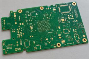
BGA stands for ball grid array. It is a surface-mount integrated-circuit package whose electrical connections are solder balls arranged in a grid on the underside of the package. During reflow, those balls join matching PCB lands. BGA supports high connection density and short interconnects, but it requires coordinated footprint, escape routing, stencil, reflow, inspection, and rework planning.
1. Define BGA by Its Connection Pattern
Traditional leaded packages place pins around the package perimeter. A BGA uses the area below the package, so it can carry far more power, ground, and signal connections within a compact outline.
| BGA element | Meaning | PCB consequence |
|---|---|---|
| Solder ball | Package terminal and solder volume | Needs a correctly sized, finished PCB land |
| Grid | Rows and columns beneath the package | Inner balls need an escape-routing strategy |
| Ball pitch | Center-to-center spacing between adjacent balls | Drives trace, via, solder-mask, and assembly capability |
| Package substrate | Routes die connections to the ball array | Adds package parasitics and affects power/thermal paths |
| Pin-1 indicator | Establishes orientation | Must agree across symbol, footprint, placement data, and assembly drawing |
Intel’s package guidance describes BGA I/O connections as being located on the interior of the device, with peripheral leads replaced by solder balls in a matrix across the bottom. That area-array architecture—not merely the presence of round solder—is the defining feature.
2. Do Not Use BGA as a Single Package Specification
“BGA” names a family. It does not define body size, pitch, ball count, ball alloy, package construction, thermal behavior, or land pattern. Even prefixes such as FBGA, FCBGA, and µBGA are not sufficient to build a footprint without the exact manufacturer drawing.
| Term | Common meaning | What still needs verification |
|---|---|---|
| PBGA | Plastic ball grid array | Pitch, body, ball alloy, moisture sensitivity, thermal data |
| FBGA | Fine-pitch ball grid array | Manufacturer definition and exact pitch |
| FCBGA | Flip-chip BGA | Die/package construction, power delivery, warpage, thermal solution |
| CSP/WLCSP | Package close to die size; may use an area array | Whether the package is technically a BGA and its board-level reliability needs |
| PoP | Package-on-package stack, often using BGA interfaces | Bottom and top interfaces, warpage, paste/flux process, stack compatibility |
TI’s package catalog alone contains many BGA configurations. The rule is simple: the orderable part number and current package drawing control the PCB footprint.
3. Compare BGA with QFN, LGA, PGA, and QFP
Community questions often ask whether BGA is “better.” That is the wrong test. BGA trades visible, easily probed leads for density, electrical performance, and a larger connection field.
| Package | Connection style | Main advantage | Main manufacturing tradeoff |
|---|---|---|---|
| BGA | Solder balls under body | High I/O density and compact routing | Joints are hidden; escape and X-ray planning matter |
| LGA | Flat lands under body | Thin package; socket or solder options exist | Solder volume comes mainly from paste and process control is critical |
| QFN | Perimeter lands plus possible exposed pad | Small and economical for moderate I/O | Bottom joints are partly hidden; thermal-pad voiding needs control |
| QFP | Gull-wing leads on perimeter | Visual inspection and hand rework are easier | Larger perimeter for high pin counts; leads can be damaged |
| PGA | Pins in a grid, often socketed or through-hole | Replaceable/socketed implementations possible | Taller, larger, and mechanically different from SMT BGA |
Choose the package supported by device availability, signal and power needs, board density, assembly volume, test access, and field-service strategy. Do not choose it from an acronym comparison alone.

4. Start the PCB Footprint with the Component Drawing
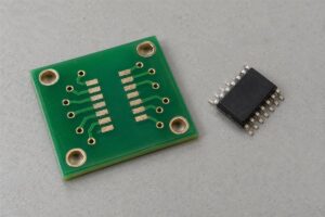
The most expensive BGA mistake is copying a land pattern from a similar-looking package. Two devices can share the same ball count and pitch while using different depopulated balls, body dimensions, package tolerances, or recommended land sizes.
| Footprint input | Source of truth | CAM/assembly check |
|---|---|---|
| Ball map and pin 1 | Device package drawing and pinout | Confirm symbol-to-footprint mapping |
| Nominal pitch | Package drawing | Measure the generated pad coordinates |
| PCB land diameter | Manufacturer recommendation, then assembly review | Check solder-mask web and fabrication tolerance |
| NSMD or SMD land | Package guidance and reliability strategy | Confirm copper/mask relationship explicitly |
| Courtyard and keepout | Package plus placement process | Include nozzle, rework, heatsink, and adjacent-part access |
| Paste aperture | Assembly/stencil engineering decision | Do not assume it always equals the copper land |
IPC-7351 provides generic land-pattern requirements, while device-specific guidance supplies the package details. When they disagree, resolve the reason with the component vendor and assembler instead of silently averaging dimensions.
5. Escape Routing Determines Whether the BGA Is Affordable
A schematic can connect every BGA ball in minutes. Routing those balls is where stackup, fabrication capability, and cost appear. Coarser arrays may escape through conventional traces and through vias; fine-pitch packages may need narrower rules, blind microvias, or filled and capped via-in-pad.
| Array condition | Likely routing approach | Question to resolve early |
|---|---|---|
| Sparse/depopulated outer rows | Dog-bone fanout and through vias | Can standard trace/space escape all required nets? |
| Dense inner rows | Additional signal layers and staggered vias | Is the proposed stackup symmetric and manufacturable? |
| Fine pitch | Microvias or via-in-pad may be needed | Are laser drill, fill, planarization, and registration qualified? |
| High-speed banks | Controlled-impedance breakouts with reference continuity | Where do return currents move during layer transitions? |
| Heavy power/ground ball count | Plane connections and distributed vias | Can the breakout also meet PDN and thermal requirements? |
Before layout, send the package drawing, ball map, proposed stackup, and breakout concept for a PCB manufacturing DFM review. A cheaper via structure is not cheaper if it leaves the inner rows unroutable.

6. Treat Via-in-Pad as a Fabrication Process, Not a Checkbox
An open via placed in a BGA pad can wick solder away from the joint. That may cause insufficient solder, voiding, or an uneven package. Proper via-in-pad solutions normally require a specified fill and a planarized cap compatible with the selected surface finish.
| Via choice | Benefit | Main risk or requirement |
|---|---|---|
| Dog-bone via outside pad | Simpler fabrication and visible geometry | Consumes breakout space |
| Tented via near pad | May reduce exposed openings | Tenting is not the same as filling a via-in-pad |
| Filled and capped via-in-pad | Direct breakout and better density | Requires qualified fill, planarization, plating, and inspection |
| Stacked microvia | Compact vertical connection | Reliability must be evaluated for stack height and process |
| Staggered microvia | Reduces stacked-interface risk in some designs | Uses more routing area and layers |
The drawing must state the required via structure. “VIP” in an email is not enough for procurement, CAM, inspection, or future supplier transfer.
7. BGA Assembly Is a Process Window
BGA balls self-align to a degree during reflow, but self-alignment does not rescue a bad footprint, excessive paste variation, warped package, poor moisture handling, or an unsuitable thermal profile. Fine-pitch devices narrow the margin further.
| Assembly input | What must be controlled | Failure if ignored |
|---|---|---|
| Storage and moisture handling | Package MSL instructions and exposure time | Package damage, delamination, or popcorning |
| Stencil and paste | Aperture, paste type, release, and print consistency | Opens, bridges, or inconsistent collapse |
| Placement | Orientation, support, accuracy, and package condition | Misalignment or wrong rotation |
| Reflow profile | Paste and component limits, board thermal mass | Incomplete wetting, excessive intermetallic growth, or warpage defects |
| Board support | Panel and local support during print/reflow | Board deflection and uneven joints |
| Cleanliness | Flux system and product requirements | Residue-related leakage or corrosion risk |
TI’s 0.5 mm package-on-package guidance calls out pad design, via-in-pad, stencil, solder paste, and coordination among the component supplier, PCB designer, fabricator, and assembler. That same cross-functional discipline applies to ordinary fine-pitch BGA work.
8. You Cannot Accept a BGA by Looking at the Top
Most solder joints are hidden under the body. External alignment and package seating can be checked visually, but joint quality normally needs process evidence and appropriate inspection—not optimism.
| Verification method | What it can reveal | Important limitation |
|---|---|---|
| 2D X-ray | Bridges, missing balls, gross void patterns, some alignment issues | Overlapping structures can hide depth information |
| Oblique/3D X-ray or CT | More spatial detail for complex defects | Higher cost, time, and interpretation needs |
| Endoscope | Accessible edge rows and package standoff | Cannot see the full array |
| Electrical test | Opens, shorts, and functional behavior | A marginal joint may pass today |
| Dye-and-pry/cross-section | Destructive evidence of interface failure | Sample-based and not for shipped units |
| Process records | Paste inspection, profile, placement, X-ray, lot traceability | Only useful when limits and reaction plans are defined |
IPC-7095E focuses specifically on BGA design and assembly implementation, including inspection, rework, and reliability. Acceptance criteria should be tied to the applicable contract documents, including the selected revisions of J-STD-001 and IPC-A-610 where required.
9. Plan Rework Before Placement
BGA rework is possible, but it is not equivalent to touching up a gull-wing lead. The rework station must heat the package and board in a controlled way, remove the device without pad damage, clean and prepare the site, place the replacement, and verify the hidden joints.
| Rework design question | Why it matters | Better decision |
|---|---|---|
| Is there nozzle clearance? | Nearby tall parts can block hot-gas tooling | Reserve a rework envelope in placement |
| Can the board be supported? | Local heating can warp large or thin boards | Define support and bottom-heater access |
| Are heat-sensitive parts nearby? | Rework exposes adjacent parts to another thermal cycle | Set shielding/removal rules and cycle limits |
| Is underfill used? | Removal can become destructive or impractical | Decide repairability before specifying underfill |
| How will replacement be verified? | Hidden joints cannot be visually touched up | Define X-ray and electrical acceptance |
If field repair matters, package selection is a serviceability decision as much as an electrical one.
10. Use This BGA Design Release Checklist
| Release check | Pass condition | Action when it fails |
|---|---|---|
| Exact package identified | Orderable part number and drawing revision are recorded | Stop footprint work until confirmed |
| Library mapping verified | Pin 1, ball names, depopulation, and coordinates match | Perform independent symbol/footprint audit |
| Stackup supports escape | Every required ball has a feasible route and reference path | Revise layers, pitch choice, or via technology |
| Fabrication rules confirmed | Pads, mask webs, traces, drills, fills, and registration pass DFM | Obtain documented capability and adjust layout |
| Assembly rules confirmed | Stencil, paste, profile, support, and MSL plan exist | Review with the assembler before release |
| PDN and thermal paths checked | Planes, vias, decoupling, and thermal solution meet analysis | Iterate placement and stackup |
| Inspection defined | X-ray/test limits and reaction plan are documented | Add measurable acceptance criteria |
| Rework evaluated | Tool access, heat exposure, and verification are feasible | Change placement or classify as nonrepairable |
| Files are complete | Gerber/ODB++, drill, stackup, BOM, XY, drawings, and notes agree | Resolve discrepancies before quotation |
For a fine-pitch or high-ball-count device, coordinate PCB fabrication and assembly support before freezing the stackup. After routing, a final CAM and assembly-data review should verify the land pattern, solder-mask data, via construction, pin-1 orientation, and manufacturing notes as one system.
Frequently Asked Questions
What does BGA stand for in electronics?
BGA stands for ball grid array, a surface-mount package with solder-ball terminals arranged in a grid beneath the component.
Is BGA a chip or a package?
BGA is a package/interconnection style. The silicon device sits inside or on the package, while the solder-ball array connects the package to the PCB.
What is the difference between BGA and FBGA?
FBGA generally means fine-pitch ball grid array. The label alone does not define one universal pitch, so use the exact package drawing and manufacturer recommendations.
Can BGA solder joints be visually inspected?
Only the outer edges may be partly visible. X-ray, electrical test, process controls, and sometimes destructive analysis are used because most joints are hidden beneath the package.
Does every BGA require via-in-pad?
No. Pitch, ball-map depopulation, trace/space capability, layer count, and net assignment determine the escape method. Coarser BGAs can often use dog-bone fanout and conventional vias.
Final Takeaway
To define BGA correctly: it is a ball grid array surface-mount package with underside solder balls arranged in a matrix. For engineering work, add the exact package drawing, pitch, ball map, land pattern, escape routing, assembly process, inspection method, and rework plan. The acronym is simple. Building a reliable BGA assembly is a coordinated PCB decision.
Sources
- IPC-7095E — Design and Assembly Process Guidance for Ball Grid Arrays
- IPC Board Design Standards — IPC-7095 and IPC-7351
- IPC — J Revisions of J-STD-001 and IPC-A-610
- Intel/Altera AN 114 — Board Design Guidelines for Programmable Device Packages
- Texas Instruments — BGA Package Portfolio
- Texas Instruments — PCB Design Guidelines for 0.5 mm Package-on-Package