Chip Antenna vs PCB Antenna: What Actually Changes?
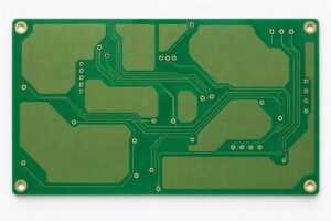
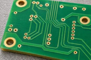
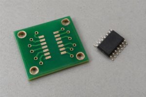
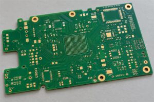
A chip antenna is a separate surface-mounted component; a printed PCB antenna uses a copper pattern on the board as its radiating structure. Choose between them by comparing the complete layout, integration effort and measured performance in the product, not just the antenna’s visible size or purchase price.
This comparison concerns an antenna printed on the main circuit board, rather than a separate cable-connected PCB antenna. Neither option has a universal range advantage. Both need an appropriate feed, surrounding geometry and a verification plan.

| Decision | Chip antenna | Printed PCB antenna |
|---|---|---|
| Physical implementation | A specified part mounted on a land pattern | A controlled copper pattern in the board artwork |
| Space to compare | Part, pads, clearance, matching and supporting board geometry | Radiating pattern, clearance, matching and supporting board geometry |
| Purchasing concern | Part availability, approved alternatives and assembly | Board area, fabrication definition and revision control |
| Design starting point | Selected part’s integration guide and reference layout | Suitable printed-antenna reference design |
| Release evidence | Verified performance of the integrated product | Verified performance of the integrated product |
A useful first decision is therefore not “Which technology is best?” but “Which implementation can we fit, tune, source and verify within this product’s constraints?” That turns an abstract comparison into a board-release decision.
Which Option Uses Less Board Space?
Compare the complete reserved antenna region, not a component body against a copper outline. A small chip can still need clearance and a suitable ground arrangement that limit where other parts may go.
The precise rules depend on the chosen antenna. For example, TI’s CC3120/CC3220 layout guide calls for antenna placement according to the manufacturer and clearance across the relevant board layers. Its recommendations belong to those implementations; do not turn them into one keepout dimension for every chip antenna.
- Draw the reserved region for each candidate. Include pads, copper exclusions, matching components and prohibited nearby objects.
- Check every layer. A top-layer opening is insufficient when the selected design requires an all-layer copper exclusion.
- Place the real mechanical parts. Add the battery, shield, display, connectors, fasteners and enclosure walls to the review.
- Check the usable board edge. Confirm that the proposed antenna location can coexist with the product’s assembly and mounting arrangement.
- Compare the resulting product outlines. Record whether either choice actually changes PCB or enclosure size.
Planning example: if two candidates both fit within an already unused edge region without enlarging the board, the smaller component body alone has not produced a PCB-area saving. If one candidate forces the connector to move or the board to grow, include that consequence in the comparison. Use actual candidate drawings; these are decision questions, not assumed antenna dimensions.
For printed designs, Silicon Labs AN1088 explains that the board and ground geometry affect its reference antenna. Copying only the visible trace while changing the rest of the implementation is not the same as reproducing the reference design.
How Should You Compare Cost and Development Effort?
Compare total incremental cost over the expected production quantity. A printed radiator removes a purchased antenna part, but it does not remove board-area, development or validation costs.
Use the following worksheet structure when comparing actual proposals. Keep shared costs out of the difference, and record which entries remain estimates.
| Cost item | Question to answer | Input to obtain |
|---|---|---|
| Antenna part and placement | What does the chip implementation add per unit? | Supplier and assembly quotes |
| PCB area or panel utilization | Does either implementation change the fabricated board cost? | Quotes for both actual outlines |
| Matching components | What is populated after tuning? | Released RF BOM, not placeholder values |
| Engineering and prototypes | How much additional work does each candidate need? | Quoted or budgeted nonrecurring effort |
| Validation and change risk | What must be retested after a layout or part change? | Agreed test scope and revision plan |
Illustrative arithmetic, not a market quote: suppose the printed option needs $900 more nonrecurring work, but its total recurring cost is $0.15 lower per unit after counting all differences. The simple break-even quantity is $900 / $0.15 = 6,000 units. At 2,000 units it saves $300 in recurring cost but still costs $600 more overall. At 10,000 units it saves $1,500 recurring and $600 overall. This comparison assumes both options meet the same requirements and ignores financing, schedule and future redesign costs.
Replace every assumed number with project evidence before choosing. If the recurring difference is zero or negative, this particular break-even argument does not favor the printed option. Silicon Labs likewise cautions that a larger board can change the apparent savings of a printed antenna.
What Must Be Tuned and Tested Before Choosing a Winner?
Check impedance matching and radiated performance as separate questions, then verify the application link in representative use. A good match is useful, but it does not prove useful radiation in every direction.

Matching means adjusting the RF connection so less power is reflected at the chosen interface. Radiation performance describes how effectively and in which directions the integrated antenna radiates. Losses and pattern nulls can still matter even when the port appears well matched. Taoglas’ integration service description treats tuning and radiation characterization as distinct parts of product development.
| Check | What it helps establish | What it does not establish alone |
|---|---|---|
| Calibrated impedance/S11 measurement | Match across the required frequency range at the defined reference plane | Radiation efficiency, pattern or final range |
| Radiation characterization | Efficiency and directional behavior under the test setup | All real installation conditions or regulatory approval |
| Application link test | Performance with the selected radio, settings and environment | Universal distance in other buildings or orientations |
| Repeat-build verification | Whether the released implementation remains consistent | That an unreviewed substitution will behave identically |
A practical prototype sequence is:
- Define the operating bands and product-level pass criteria before measuring.
- Reserve the matching and test-access arrangement recommended for the selected design.
- Measure with a documented, calibrated setup and defined reference plane; account for test-fixture effects.
- Tune and recheck with the intended battery, enclosure and nearby mechanical parts present.
- Verify radiated behavior and representative orientations, then run repeatable application tests.
- Freeze the accepted layout, materials, antenna part and populated matching values together.
TI specifically recommends tuning with the complete assembly and casing because they can affect impedance. Taoglas’ chip-antenna application note also shows why matching values are implementation-dependent. Do not copy another board’s capacitor and inductor values as a guaranteed final solution.
For a fair A/B trial, record board revision, enclosure, firmware, radio settings, test position and orientation for both candidates. Change one controlled variable at a time. A one-off walk test with different battery states or receiver positions cannot isolate the antenna choice.
What Should You Send for PCB Design and Manufacturing Review?
Send the complete antenna integration definition, including the mechanical environment and validation responsibilities. A part number or screenshot alone cannot define the finished RF implementation.
- Electrical target: operating bands, radio interface and agreed performance criteria.
- Antenna definition: exact component and integration guide, or controlled printed pattern and reference source.
- Board definition: fabrication data, approved stackup, relevant material properties, thickness and RF feed requirements.
- Clearance: layer-specific keepouts and restricted nearby components or metalwork.
- Mechanical context: enclosure, battery, connectors and intended antenna position.
- Assembly definition: BOM, antenna orientation, matching footprints and released population options.
- Verification plan: who tunes, who performs RF testing, and which changes require reassessment.
Use a PCB design review to resolve missing layout information before fabrication. Ask the PCB manufacturing team to confirm the controlled stackup and geometry it will build. RF performance approval remains a separate responsibility unless the quoted service explicitly includes it.
FAQ
Does a chip antenna always give longer range?
No. Compare measured integrated performance under the same radio settings, enclosure and test conditions. The component category alone does not determine the link.
Is a printed PCB antenna free?
It has no separate purchased radiator, but additional board area, engineering and validation can carry costs. Compare complete proposals rather than the antenna BOM line alone.
Can I put components in the antenna keepout?
Follow the selected design’s restrictions. Do not reclaim the reserved space without an integration review and appropriate revalidation.
Can I replace a chip antenna with one of the same size?
Not on size alone. Compare the integration requirements, frequency coverage, land pattern and behavior, then review and validate the alternative before release.
Can both options need matching components?
Yes. The required network and values depend on the implementation. Reserve suitable provisions during layout instead of assuming the first prototype will need none.
Should I tune with the enclosure removed?
An open-board measurement can be useful diagnostically, but the final decision should represent the product’s intended assembled environment.
Is good S11 enough to approve the antenna?
No. It answers a matching question, not the entire radiation or application-performance question. Use the other tests required by your product specification.
What if neither antenna fits the product constraints?
Revisit the mechanical layout or evaluate another antenna arrangement with an RF specialist. Do not force an unsuitable reference layout into the board and assume tuning will repair every limitation.
To review the PCB implementation, contact QFPCB with the files and requirements above. Ask for confirmation of the proposed build and clearly separate fabrication checks from antenna tuning and RF acceptance testing.