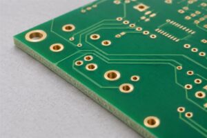
“Use a ceramic PCB whenever the board runs hot.” That advice is easy to repeat and expensive to apply blindly. Ceramic can improve heat flow, electrical isolation, dimensional stability, and high-temperature performance—but only when the substrate, metallization, copper thickness, attachment method, and cooling path match the application.
Direct answer: A ceramic PCB uses an electrically insulating ceramic substrate—commonly alumina, aluminum nitride, or silicon nitride—with patterned conductors formed by thick film, thin film, direct bonded copper, active metal brazing, or a co-fired multilayer process. It is selected for power density, thermal cycling, high-frequency precision, hermetic packaging, or high-temperature operation. The right choice depends on thermal resistance, CTE, mechanical strength, dielectric behavior, conductor geometry, assembly process, reliability target, and cost.

A Ceramic PCB Is Not Just “Better FR-4”
FR-4 is a laminated composite that supports plated holes, multilayer routing, fine digital interconnects, and economical panel processing. A ceramic circuit is a different manufacturing system. The ceramic may carry printed and fired metal, deposited thin film, bonded copper, brazed copper, or co-fired internal conductors.
Also, a hydrocarbon or PTFE laminate filled with ceramic particles is still a polymer-based laminate. It should not be specified as a solid ceramic substrate.
The useful question is not “Is ceramic better?” It is “Which failure mechanism or performance limit requires ceramic?”
Why Ceramic PCB Projects Get Stuck
Community discussions often begin with thermal conductivity and skip the rest of the stack.
- Pain: unexpected cracking, delamination, copper lift, solder-joint fatigue, warped substrates, expensive minimum quantities, or a design that cannot be fabricated at the requested geometry.
- Difficulty: material properties vary by grade, temperature, thickness, metallization, and supplier process; one headline conductivity value does not describe the assembled thermal path.
- Decision barrier: buyers do not know whether they need alumina, AlN, Si₃N₄, thick film, thin film, DBC, AMB, LTCC, or an ordinary metal-core PCB.
Start with function and reliability. The process choice follows.

Ceramic PCB Material Comparison
| Material | Why designers choose it | Main trade-off | Typical fit |
|---|---|---|---|
| Alumina (Al₂O₃) | Mature, electrically insulating, mechanically stable, cost-effective for ceramic | Lower thermal conductivity than AlN; brittle | LED modules, sensors, hybrid circuits, general power electronics |
| Aluminum nitride (AlN) | High thermal conductivity and CTE closer to silicon | Higher cost; processing and handling require control | Power modules, laser diodes, high-heat semiconductor submounts |
| Silicon nitride (Si₃N₄) | Strong mechanical and thermal-cycling performance | Cost and supplier/process availability | Automotive and high-reliability power modules |
| Zirconia-toughened alumina | Improved toughness over conventional alumina | Thermal and cost balance is grade-specific | Power substrates requiring added cycling robustness |
Rogers publishes product-specific DBC examples using alumina, zirconia-toughened alumina, and AlN with different thermal conductivity and CTE values. Those numbers are useful for comparing that product family, not as universal constants for every ceramic grade.
1. Thick-Film Ceramic Circuits
Thick-film processing screen-prints conductive, resistive, or dielectric pastes onto ceramic and fires them at high temperature. It supports hybrid circuits, printed resistors, multiple conductor layers, and cost-effective repeated patterns.
Kyocera describes thick-film conductors as screen-printed conductive paste and shows how multilayer ceramic structures can be laminated and co-fired. The process is established, but geometry, resistance, surface roughness, paste system, firing profile, and solderability must be specified with the supplier.
Use thick film when its feature size and electrical performance meet the design. Do not request thin-film geometry from a thick-film cost structure.

2. Thin-Film Ceramic Circuits
Thin-film processes use vacuum deposition or sputtering, patterning, and plating to create fine, accurately positioned conductors on a polished ceramic surface. They are useful for RF, microwave, optical, sensor, and precision resistor applications.
Kyocera notes that thin-film processing can produce finer, higher-precision patterns than screen-printed thick film and can combine deposited stacks with thicker plated copper where current or heat spreading requires it.
The trade-off is process complexity and cost. Surface finish, adhesion layer, conductor stack, line geometry, resistor trim, plating, and wire-bond requirements all need early agreement.
3. Direct Bonded Copper (DBC)
DBC bonds relatively thick copper to alumina or AlN using a high-temperature process. It gives power devices a low-resistance conductor, electrical isolation through ceramic, and a direct route toward a baseplate or cooler.
Rogers describes DBC as pure copper bonded to a ceramic isolator and provides process-specific design rules for ceramic and copper thickness, conductor width, spacing, surface finish, and peel strength.
DBC is not routed like ordinary thin copper. As copper thickness increases, practical etched feature width and spacing also grow. Copper geometry, ceramic thickness, edge clearance, stress relief, and thermal cycling must be designed together.
4. Active Metal Brazed (AMB) Substrates
AMB uses an active braze system to join copper to ceramic. It is often associated with silicon nitride and high-reliability power modules where mechanical robustness and thermal cycling matter.
Do not choose AMB from a marketing label alone. Compare substrate strength, copper attachment, conductor geometry, void control, thermal resistance, surface options, cycling evidence, and supplier design rules against the actual mission profile.
5. LTCC and HTCC Multilayer Ceramics
Low-temperature and high-temperature co-fired ceramics build conductors and vias into stacked ceramic tape before firing. They can create compact three-dimensional interconnect, embedded passives, cavities, packages, and hermetic structures.
The shrinkage, conductor material, via rules, layer alignment, firing process, and design library are supplier-specific. Moving an FR-4 multilayer layout into LTCC is not a file-format conversion; it is a new substrate design.
Thermal Conductivity Is Not Thermal Performance
A high-conductivity substrate helps only if heat can enter it and leave it. Calculate or simulate the complete path:
junction → die attach/solder → copper or film → ceramic → interface material → heat spreader/cooler → ambient
Include spreading resistance, interface voids, copper area, substrate thickness, mounting pressure, baseplate flatness, coolant or airflow, and nearby heat sources. A thin ceramic with a poor interface can perform worse than a modest material with a well-controlled attachment.
For a new project, an early ceramic PCB engineering review should begin with loss maps, isolation requirements, mechanical constraints, cycling profile, and the proposed cooler—not merely the desired substrate conductivity.
CTE and Thermal Cycling Decide Reliability
Ceramic is brittle, while copper, solder, baseplates, and packages expand differently. Repeated temperature changes create shear and bending stresses. Large uninterrupted copper regions can make the substrate behave asymmetrically and increase stress near edges, corners, and die locations.
Review:
- ceramic and copper thickness;
- copper balance on both sides;
- die and baseplate CTE;
- solder or sinter attachment;
- copper edge shape and stress-relief geometry;
- substrate size and mounting method;
- temperature range, dwell, and ramp;
- power cycling separately from ambient cycling.
Reliability data must match the construction. “Ceramic survives high temperature” does not prove a bonded copper assembly survives repeated power cycling.
Electrical Design Still Matters
Ceramics offer high insulation capability, but layout controls the real electric field. Define operating voltage, transient voltage, pollution environment, altitude, conductor finish, edge conditions, and required test method.
For RF and high-speed circuits, obtain process-specific dielectric constant, loss, thickness tolerance, conductor profile, and surface roughness. Do not reuse an FR-4 impedance model. Thin-film and thick-film conductors also have different resistivity and geometry from etched copper.
Design Rules Must Come From the Selected Process
Before layout, request a supplier capability table covering:
- ceramic materials, grades, and available thicknesses;
- metallization or bonded-copper processes;
- conductor thickness, minimum width, spacing, and edge clearance;
- holes, slots, laser features, tolerances, and edge quality;
- single- or double-sided routing and via options;
- surface finishes and wire-bond compatibility;
- solder mask or dielectric overcoat options;
- substrate size, panelization, flatness, and bow;
- electrical, dimensional, and visual inspection;
- sample, qualification, and production lot controls.
A proper CAM and DFM review for ceramic substrates checks the design against the exact process route. Generic PCB rules are not enough.
Assembly Requires a Ceramic-Specific Plan
Ceramic handles heat differently and tolerates less mechanical bending than an organic board. Review stencil support, reflow profile, fixture contact, pick-and-place force, depaneling, cleaning, underfill, wire bonding, die attach, and inspection.
Large or heavy components can load a brittle substrate during vibration. Thermal mass can create soldering gradients. Bare-die processes add surface cleanliness, metallization, attach voiding, bondability, and contamination requirements.
For turnkey production, the PCB fabrication and assembly package should link substrate revision, metallization, finish, attachment materials, component handling, thermal profile, inspection criteria, and test limits.
Ceramic PCB vs Metal-Core PCB
| Decision | Ceramic substrate | Metal-core PCB |
|---|---|---|
| Electrical isolation | Ceramic itself is the dielectric | Thin polymer dielectric separates copper from metal core |
| Thermal path | Material/process dependent; can be excellent | Often cost-effective for spreading heat to aluminum base |
| Fine multilayer routing | Limited or process-specific | More familiar PCB-style options, still construction-dependent |
| Mechanical behavior | Hard and brittle | Metal core is tougher but CTE and dielectric limits remain |
| Cost | Usually higher and more specialized | Often lower for LED and moderate-power applications |
| Best use | High power density, precision, high temperature, bare die | Cost-sensitive heat spreading with conventional assembly |
If a metal-core board meets the junction-temperature, isolation, size, and reliability target, ceramic may add cost without adding product value.
Saveable Ceramic PCB RFQ Checklist
- Application and mission profile.
- Ceramic material, grade, thickness, and allowed substitutions.
- Manufacturing process: thick film, thin film, DBC, AMB, LTCC, or HTCC.
- Copper/metallization stack and thickness.
- Electrical isolation and test voltage requirements.
- Thermal loss map, attachment, cooler, and target temperatures.
- Conductor width, spacing, edge distance, and finish.
- Mechanical dimensions, flatness, holes, slots, and tolerances.
- Die attach, solder, sinter, wire-bond, or component assembly process.
- Thermal cycling, power cycling, vibration, and qualification plan.
- Inspection, electrical test, traceability, and sample reports.
- Prototype quantity, production volume, yield assumptions, and revision control.
Do not request a quote with only dimensions, layer count, and “AlN.” That is not enough to define the product.
Frequently Asked Questions
What is a ceramic PCB made of?
It uses a ceramic electrical insulator such as alumina, aluminum nitride, or silicon nitride with patterned metal conductors. The conductor may be printed and fired, deposited, plated, directly bonded, brazed, or co-fired inside a multilayer structure.
Is aluminum nitride always better than alumina?
No. AlN generally offers higher thermal conductivity, but alumina is mature, widely available, and often more economical. Choose from complete thermal, mechanical, electrical, reliability, manufacturing, and cost requirements.
Is a ceramic PCB the same as a ceramic-filled RF laminate?
No. A ceramic-filled laminate uses ceramic particles inside a polymer system, while a ceramic PCB uses a solid ceramic substrate or co-fired ceramic body. Their processing and properties differ.
Can ceramic PCBs have multiple layers?
Yes, through processes such as LTCC or HTCC, and some thin-film or hybrid constructions can add multilayer interconnect. The rules are process-specific and differ significantly from FR-4 multilayer fabrication.
Why do ceramic substrates crack?
Common causes include mechanical shock, bending, poor fixturing, edge damage, unbalanced copper, attachment stress, CTE mismatch, thermal gradients, and repeated cycling. Material strength alone does not eliminate assembly-induced stress.
Final Takeaway
A ceramic PCB is valuable when the application needs its thermal, dielectric, dimensional, or high-temperature behavior enough to justify a specialized process. Select the ceramic and metallization together, model the full thermal path, design for CTE stress, and obtain process-specific rules before layout. Save the RFQ checklist; it will prevent more problems than choosing material from one conductivity number.