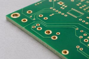
“Choose the ceramic with the highest thermal conductivity.” That is not a material-selection method. It ignores fracture toughness, copper attachment, coefficient of thermal expansion, dielectric behavior, processing, supply, cost, and the thermal resistance outside the substrate. The best ceramic circuit board material is the one that survives the complete electrical, thermal, mechanical, and manufacturing mission profile.
Direct answer: Alumina is usually the cost-effective default for ceramic circuits. Aluminum nitride is preferred when heat spreading and CTE compatibility with silicon dominate. Silicon nitride is strong and tough for severe thermal and power cycling. Zirconia-toughened alumina improves mechanical robustness while retaining an alumina-based process. Beryllium oxide offers specialized thermal performance but carries serious occupational-health controls if dust is generated. Select a supplier grade and metallization process—not only a chemical name.

Why the Material Name Is Not a Specification
“96% alumina,” “AlN,” or “Si₃N₄” does not define the finished circuit carrier. Purity, additives, grain structure, porosity, firing, surface finish, thickness, flatness, metallization, bonded copper, plating, and machining all affect performance.
Published numbers also use different temperatures and test methods. Kyocera’s material-property tables and CeramTec’s substrate comparison show that properties are tied to particular grades. Treat supplier data as design input for that product, not a universal constant.
Ceramic Circuit Board Material Comparison
| Material | Main strength | Main limitation | Best first look |
|---|---|---|---|
| Alumina, Al₂O₃ | Mature, insulating, broadly available, favorable cost | Moderate thermal conductivity and brittleness | General hybrid circuits, LEDs, sensors, moderate-power modules |
| Aluminum nitride, AlN | High thermal conductivity and CTE close to silicon | Higher cost and more specialized processing | Lasers, RF power, high-heat semiconductor submounts |
| Silicon nitride, Si₃N₄ | High strength, toughness, and cycling capability | Cost, availability, and process-specific metallization | Automotive and high-reliability power modules |
| ZTA/HPS | Tougher alumina-family option | Thermal advantage over alumina may be limited | DBC where cycling robustness needs improvement |
| Beryllium oxide, BeO | Specialized combination of insulation and heat conduction | Health, machining, labeling, waste, and supply-chain controls | Legacy or tightly controlled specialist applications |
This table is a screening tool. Final selection requires product-grade data and the exact conductor-attachment process.
1. Alumina: The Default for a Reason
Alumina is widely used because it balances electrical insulation, mechanical strength, temperature capability, dimensional control, metallization compatibility, supply, and cost. It supports thick film, thin film, DBC, multilayer packages, and many hybrid processes.
Use alumina when the full thermal model meets junction-temperature limits and the mechanical profile is manageable. Do not reject it simply because AlN has a higher conductivity number. For many designs, the dominant resistance is die attach, interface material, cooler, or convection—not the ceramic.
Key decisions include purity/grade, thickness, surface roughness, flatness, hole and edge quality, and metallization. Higher purity does not automatically mean a better circuit; it can change cost, firing, surface, and processing.

2. Aluminum Nitride: Choose It for a Quantified Thermal Need
AlN combines electrical insulation with high thermal conductivity and a CTE relatively close to silicon. Kyocera identifies these properties as reasons AlN is used for heat-dissipating semiconductor substrates and packages.
The mistake is specifying AlN without a loss map. First calculate the complete path from junction through attachment, metal, ceramic, interface, cooler, and ambient. Then compare temperature and stress using actual supplier-grade values.
AlN processing also needs control. Metallization adhesion, surface preparation, laser machining, edge damage, moisture exposure during processing, and solder or braze compatibility should be agreed with the supplier. A generic alumina process cannot always be transferred unchanged.
3. Silicon Nitride: Mechanical Reliability Can Beat Peak Conductivity
Si₃N₄ is attractive for high-reliability power modules because of strength, fracture toughness, low expansion, and thermal-shock behavior. CeramTec’s product comparison positions silicon nitride above alumina and AlN in toughness and flexural strength for the listed grades, while Rogers offers Si₃N₄ in AMB constructions for power electronics.
This matters when thick copper, large dies, baseplates, vibration, and repeated power cycling create mechanical stress. A lower thermal-conductivity substrate that survives the mission can be the better choice than a higher-conductivity substrate that cracks or drives attachment fatigue.
Ask for construction-specific cycling data. Ceramic grade, thickness, copper thickness, copper geometry, braze, die attach, and test profile all affect the result.
4. ZTA: When Alumina Needs More Toughness
Zirconia-toughened alumina adds zirconia to improve fracture toughness and flexural behavior. It can provide a useful middle ground when standard alumina is mechanically marginal but the project does not require the thermal performance or cost of AlN.
ZTA is not one universal formula. Rogers identifies an HPS alumina with zirconia content in its product family, while CeramTec publishes separate ZTA grade data. Compare actual supplier grades, DBC availability, thermal conductivity, dielectric strength, CTE, thickness, copper design rules, and cycling evidence.
5. BeO: High Performance With a Non-Negotiable Safety Burden
Beryllium oxide has been used in RF and power-electronics packaging because it can combine electrical insulation with high heat conduction. It cannot be treated like an ordinary workshop ceramic.
Materion’s U.S. safety data warns against breathing dust or fumes and identifies sensitization, carcinogenicity, and respiratory-organ risks. Finished intact articles and dust-generating machining are different exposure conditions, but design, fabrication, rework, marking, breakage response, and disposal must all follow applicable controls.
Do not drill, grind, sand, laser-machine, or dispose of unknown BeO using general PCB procedures. If BeO is considered, involve the material supplier and qualified EHS professionals before design release. In many new designs, AlN or another controlled alternative is preferred even if a narrow thermal comparison favors BeO.
Thermal Conductivity: Use It Correctly
The one-dimensional substrate estimate is:
Rθ = thickness ÷ (thermal conductivity × heat-flow area)
Real boards add spreading resistance and several interfaces. Copper pattern, die size, attach voids, ceramic thickness, backside metallization, thermal interface material, clamping, cooler flatness, and airflow or coolant may dominate.
Run sensitivity cases. If changing from alumina to AlN barely changes junction temperature, spend the budget on the actual bottleneck. An early ceramic substrate engineering review should compare complete thermal stacks rather than substrate conductivity alone.
CTE: Match the Assembly, Not One Component
Low CTE mismatch can reduce stress between a silicon die and substrate, but the module also contains copper, solder or sinter, terminals, baseplate, encapsulant, and housing. Thick copper can dominate composite expansion and bending.
Evaluate:
- die size and attachment area;
- ceramic and copper thickness;
- copper balance and edge geometry;
- baseplate material and attachment;
- operating and storage temperature ranges;
- thermal ramp, dwell, and cycle count;
- power cycling versus ambient cycling;
- vibration, shock, and mounting force.
Material selection and conductor geometry must be reviewed together.
Electrical Properties Depend on Frequency and Conditions
Dielectric constant, loss tangent, insulation resistance, dielectric strength, and breakdown behavior vary with grade, frequency, temperature, thickness, surface condition, and test method. For RF, microwave, and precision circuits, request data in the relevant frequency range.
Do not use one website’s room-temperature dielectric number to close an impedance model. Obtain process-specific thickness tolerance, metallization profile, conductor roughness, and dimensional capability from the fabricator.
Manufacturing Process Can Override Material Preference
A material is useful only if available in the required process:
- thick-film printing for robust hybrid circuits and printed resistors;
- thin film for fine features, RF, optics, and precision networks;
- DBC for thick copper on alumina or AlN;
- AMB for robust copper attachment, often with Si₃N₄;
- LTCC/HTCC for co-fired multilayer interconnect and packages.
An early CAM and DFM review should confirm material grade, thickness, panel/master-card format, conductor process, holes, edge clearances, surface finish, flatness, and inspection before layout is frozen.
Saveable Material Selection Matrix
Score each candidate from 1 to 5 using verified supplier data, then weight the rows for your project.
| Criterion | Evidence required | Common mistake |
|---|---|---|
| Junction temperature | Full thermal model and measured correlation plan | Ranking conductivity only |
| CTE stress | Assembly-level FEA or validated precedent | Comparing ceramic only to die |
| Mechanical reliability | Strength, toughness, edge and cycling data | Treating all ceramics as equally brittle |
| Electrical behavior | Frequency- and temperature-relevant data | Using a generic dielectric constant |
| Metallization | Qualified thick/thin film, DBC, or AMB route | Selecting material before process |
| Geometry | Supplier width, spacing, holes, flatness, thickness rules | Applying FR-4 capabilities |
| Assembly | Attach, reflow, wire bond, fixture and cleaning plan | Ignoring ceramic handling |
| Safety/EHS | SDS, machining, rework and disposal controls | Treating BeO like alumina |
| Supply | Grade lifecycle, source, MOQ, lead time, change control | Specifying an unavailable grade |
| Cost/yield | Prototype and volume assumptions | Comparing raw substrate price only |
Questions to Put on the RFQ
- What exact ceramic grade and manufacturer will be supplied?
- Which properties are guaranteed and which are typical?
- At what temperature, frequency, and test method were values measured?
- What metallization or copper-bonding process is qualified?
- Which material/thickness/copper combinations are standard?
- What are the edge, hole, flatness, bow, and surface specifications?
- What thermal- or power-cycling evidence matches this construction?
- Which operations occur after metallization and how are parts cleaned?
- What inspection, electrical test, traceability, and certificate data are available?
- How are material or process changes communicated?
For assembly projects, link these answers to the PCB fabrication and assembly specification so the substrate, finish, die attach, solder, wire bond, inspection, and test revisions cannot drift apart.
Frequently Asked Questions
What is the most common ceramic circuit board material?
Alumina is the common general-purpose choice because of its established processing, electrical insulation, availability, and cost-performance balance. High heat density or severe cycling may justify AlN, Si₃N₄, or ZTA.
Is AlN always the best material for heat dissipation?
No. It offers high thermal conductivity, but complete thermal-path resistance, CTE stress, toughness, metallization, geometry, supply, yield, and cost determine system performance.
Why is silicon nitride used in power modules?
Its strength, fracture toughness, low expansion, and thermal-shock behavior can improve reliability under vibration and repeated thermal or power cycling. The benefit must be validated for the full AMB/copper/module construction.
Can BeO ceramic boards be handled safely?
Intact finished articles and dust-generating processing present different conditions, but BeO requires formal hazard controls. Never machine, abrade, break, rework, or discard it without supplier SDS guidance and qualified EHS procedures.
Can ceramic material values be used directly in simulation?
Use only data for the selected supplier grade and relevant conditions. Document whether each value is typical or guaranteed, then correlate the model with prototype measurements.
Final Takeaway
Choosing a ceramic circuit board material is not a contest for the highest conductivity. Alumina often wins on balanced cost and process maturity; AlN on heat flow and silicon compatibility; Si₃N₄ on mechanical and cycling reliability; ZTA on tougher alumina-family performance; and BeO only in specialist, tightly controlled cases. Select the material, metallization, assembly, and qualification route as one system—and save the matrix before requesting quotes.