What Two Extra Copper Layers Actually Change

Choose a 6 layer PCB when the design routes cleanly with suitable reference planes and a manufacturable stackup. Choose an 8 layer PCB when the extra layers solve a demonstrated routing, reference-plane or power-distribution constraint. Eight layers are not automatically faster or more reliable, and six layers are not automatically cheaper after redesign and qualification costs.
The layer count describes conductive copper layers, not the number of insulating sheets. Some copper layers carry signals; others distribute power or provide ground references. Therefore, moving from six to eight does not necessarily give you two extra signal-routing layers. One added layer may be needed as a reference plane for the other.
In plain language, a reference plane is the nearby copper surface that helps a signal complete its electrical loop. Counting routes without accounting for their return paths is an incomplete comparison. Altium’s stackup introduction explains these layer roles and gives example six- and eight-layer arrangements. Those examples are starting points, not fabrication-ready constructions.
| Decision item | Six-layer candidate | Eight-layer candidate | Evidence to compare |
|---|---|---|---|
| Routing capacity | May be adequate after good placement | Can provide additional usable routing space | Trial routing at approved width, spacing and via rules |
| Plane allocation | Less room for independent plane assignments | More flexibility, depending on actual allocation | Layer-purpose map and reference-plane continuity |
| Mechanical envelope | Must meet the specified thickness and tolerance | Can meet the same nominal thickness with another construction | Fabricator’s finished stackup, not layer count alone |
| Project cost | Potentially lower bare-board price | Potentially less routing pressure or redesign work | Comparable quotations plus engineering and test scope |
Decide from Routing and Return Paths, Not Clock Frequency
The useful question is whether the actual interfaces can be routed and verified, not whether the clock crosses a particular MHz threshold. A slow repetition rate can still have fast switching edges. Texas Instruments’ High-Speed Layout Guidelines discusses why edge behavior, return-current paths and discontinuities matter.
Start with the component manufacturer’s interface requirements. List the controlled-impedance nets, allowed length or delay relationships, connector constraints and return references. Also identify sensitive analog nodes, switching-power loops and densely pinned devices. This turns a vague request for an “eight-layer high-speed board” into a set of constraints that can be checked.
- Place the difficult parts first. Position the processor, memory, connectors and their supporting components within the real enclosure constraints.
- Trial-route the limiting interface. Use the proposed production trace widths, clearances and via structures. Do not declare success using rules the selected fabricator cannot build.
- Follow the reference beneath each critical route. Identify plane gaps and layer transitions. A route that connects electrically may still have an unsuitable return path.
- Record the actual reason for an upgrade. Examples include an unroutable escape region, a required extra routing channel, or a plane allocation that cannot otherwise remain continuous.
Example: imagine a compact controller where connector placement forces several critical nets through one crowded corridor. Before adding layers, test whether moving a connector or changing placement opens that corridor. If six layers still require unacceptable spacing or broken reference paths, compare an eight-layer candidate that removes those particular problems. This is a decision method, not a claim that every controller needs eight layers.
A board that passes connectivity checks has not thereby passed signal-integrity or EMC testing. Keep interface simulation and prototype validation in the plan wherever the product requirements demand them.
Stackup Checks Before You Commit to Six or Eight Layers

Approve the physical construction with the fabricator before treating the layer count as final. The same layer labels can describe different dielectric thicknesses, copper weights and material systems. They can require different routing dimensions.
Altium’s controlled-impedance documentation ties routing profiles to the layer stack and reference geometry. Consequently, do not carry trace widths unchanged from a six-layer layout into an eight-layer layout without checking the new construction.
| Review item | Question to answer | Release evidence |
|---|---|---|
| Layer assignment | What is each layer for, and what references each critical signal? | Numbered signal, ground and power layer map |
| Material and spacing | Which materials and finished dielectric distances are being used? | Supplier-approved construction and applicable tolerances |
| Impedance | Do the required widths and pair gaps fit the escape and routing regions? | Impedance table with layer, target, tolerance, width and gap |
| Vias | Can the chosen holes, pads and layer transitions be manufactured? | Drill map and DFM approval; special processing identified |
| Mechanical fit | Will the finished thickness meet connectors, slots and enclosure constraints? | Drawing with finished-thickness tolerance |
Review these items together. For example, reducing a dielectric spacing may change the width needed for a specified impedance; a narrower trace may then encounter fabrication limits. Altium’s stackup considerations discusses this interaction between electrical geometry and manufacturability.
Ask for the proposed build before routing is nearly finished. The PCB layer-stackup service information is a relevant starting point for that discussion; confirm the actual construction for your board rather than assuming a published example is your approved build.
Compare Total Build Cost with the Same Assumptions
Request two comparable quotes instead of applying a universal percentage premium to eight layers. Board dimensions, order quantity, material, drilling, copper, finish, testing and lead time can change the comparison. Supplier-specific standard constructions matter too: Eurocircuits’ published service scope, for example, distinguishes standard builds from special options. This does not establish QFPCB pricing.
| Hold equal when possible | Flag if different | Why it belongs in the comparison |
|---|---|---|
| Outline, quantity and delivery requirement | Different panel utilization or expedited schedule | A lower unit price may describe a different order |
| Material grade, copper and surface finish | Substitution or changed copper construction | Electrical and manufacturing scope may have changed |
| Testing and acceptance documentation | Impedance coupons, reports or inspection excluded | Unquoted verification still needs funding |
| Via technology and design rules | Blind vias, microvias, backdrilling or tighter geometry | The cheaper layer count can still require a more complex build |
| Engineering and qualification scope | Rerouting, a new prototype or repeat tests | Bare-board savings are not total-project savings |
Use this simple comparison: project difference = quoted board-price difference × quantity + confirmed differences in engineering, tooling and validation cost. Keep uncertain risks separate rather than assigning invented failure probabilities.
Hypothetical calculation, not a QFPCB quote: if comparable eight-layer boards cost $0.80 more each at 500 pieces, the direct difference is $400. If the six-layer alternative needs an additional 10 hours of verified routing work at an internal cost of $60 per hour, that adds $600. On those assumptions alone, the eight-layer option is $200 lower in combined board and routing cost. Different real quotes or engineering estimates can reverse that conclusion.
A Release Checklist for the Layer-Count Decision
Release the option whose technical constraints and commercial assumptions have been checked, and save the reason for the choice. A short decision record helps engineering and purchasing discuss the same board.
- Identify the selected layer count, board revision and exact stackup revision.
- Attach the critical-net requirements and trial-routing findings.
- Resolve every open return-path, impedance and via-manufacturing issue.
- Confirm finished thickness, material, copper and fabrication tolerances.
- Compare quotes with exclusions and optional processes visible.
- Name the required prototype tests and the person responsible for accepting them.
- State the reason rejected options were not selected, without claiming unperformed tests passed.
If the layer count is still uncertain, send the schematic, preliminary placement, critical-interface requirements, board outline and mechanical limits for a PCB design discussion. Once fabrication data is ready, provide the layer files, drills, stackup and impedance table. Through QFPCB’s contact page, request a six-versus-eight-layer feasibility comparison and equivalent-scope quotations. Ask what changes are required in each option before approving production.
FAQ
Can I identify six or eight layers by looking at the board?
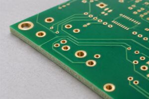
Not reliably from a normal surface photograph. Check the fabrication drawing and approved stackup. An edge view is not a dependable acceptance method for counting every thin internal copper feature; use appropriate manufacturing records or agreed inspection evidence.
Does eight layers mean the finished board must be thicker?
No. Different constructions can target the same finished thickness. Whether that construction meets your impedance, copper, drilling and mechanical requirements must be confirmed with the fabricator.
Can I keep the same Gerber files when changing layer count?
Do not treat this as an automatic conversion. New assignments can require rerouting, updated plane data, drill changes and new impedance dimensions. Release a consistent fabrication package tied to the revised stackup.
Are microvias mandatory on an eight-layer PCB?
No. Layer count alone does not specify via technology. Component escape geometry and routing requirements determine whether ordinary through-holes are adequate or more advanced structures are needed. Ask the fabricator to review the actual design.
Will an eight-layer board pass EMC tests automatically?
No. More layers can help implement a better layout, but connectors, cables, return paths, filtering, enclosure design and component behavior still matter. Compliance requires the appropriate product-level evaluation.
Can a six-layer prototype validate an eight-layer production board?
It can help evaluate functionality, but it does not fully qualify a changed stackup. Review which electrical, mechanical and manufacturing characteristics changed and repeat the tests affected by those changes.
Should I reserve spare layers for future revisions?
Only with a documented reason. Future routing flexibility may be useful, but unused capacity has a cost and still needs a sensible stackup. Compare a known product roadmap against the present build rather than adding layers by habit.
What should purchasing ask if two suppliers suggest different layer counts?
Ask each supplier to identify the constraint their proposal solves, provide the proposed stackup and state the required layout changes. Then compare equivalent materials, rules, testing and quantities. A bare layer count is not enough to compare offers.